 Products Home / Technical Resources / Electro-Optic Modulator Technical Publications / Free-Space Electro-Optic Modulators Tutorial
Free-Space Electro-Optic Modulators Tutorial


Please Wait

Introduction to Electro-Optic Modulators
- Introduction
- Static Phase Retardance (SPR)
- EO Phase Modulator
- EO Polarization Modulator
- EO Amplitude Modulator
- Effect of SPR in Amplitude Modulators
- Amplitude Modulator Compensation
- Compensation Methods
- Temperature-Independent Amplitude Modulator
- Operation in the Thorlabs Housing
- Driving EO Modulators
Click for Details
Figure 1: A schematic of a typical X-cut LN crystal used for EO modulators is displayed.
Introduction
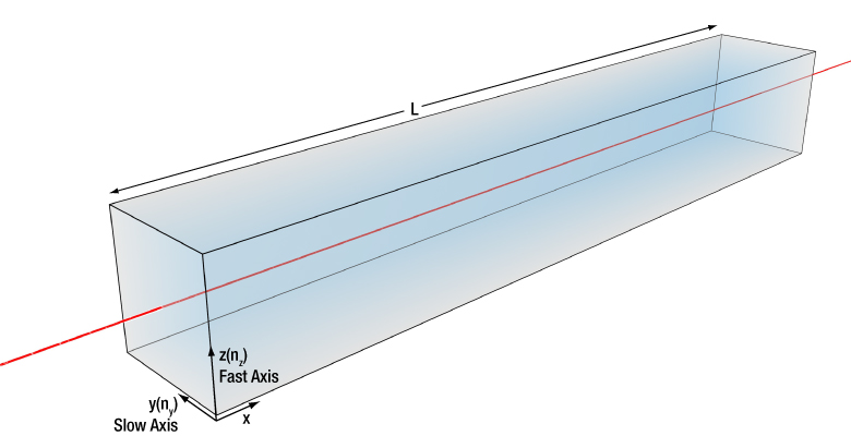
Thorlabs' free-space electro-optic (EO) modulators enable users to modulate free-space optical beams at speeds up to 100 MHz. They are based on MgO-doped lithium niobate (LN), which is known for its efficient EO response and utility over a broad range of wavelengths. LN is a birefringent, uniaxial EO crystal typically used in the geometry depicted in Figure 1. The crystal is cut, with respect to the crystalline axes, for optical propagation along the x-axis with a driving voltage applied across the z-axis. This gives the highest EO response for both phase and amplitude modulators. In the following text, we describe the basic principles involved and how they lead to use of this crystal in phase, polarization, and amplitude modulators.
The crucial aspect of this crystal geometry is that light is only allowed to propagate with two orthogonal linear polarizations along the crystal’s y-axis and z-axis. Since the crystal is birefringent, the two polarizations will experience different optical indices, ny and nz , and will therefore travel at different speeds. The difference between the indices, (ny - nz), is denoted by Δn. For LN, ny is greater than nz , so light polarized along the y-axis (slow axis) travels slower than along the z-axis (fast axis). As a result, when light enters the crystal the two orthogonal linear polarizations will travel at different speeds and exit the crystal with a phase difference corresponding to the optical path difference, which is Δn times the crystal length, L.
Static Phase Retardance (SPR)
The phase difference resulting from the crystal’s inherent Δn is commonly known as the static phase retardance, and is represented here as SPR. The SPR is a function of Δn, the wavelength, λ, and crystal length, L. The factor of 2pi gives the SPR in radians while the factor of 360, in the alternate equation, provides it in degrees.
SPR (radians) = 2pi ⋅ Δn ⋅ L / λ or SPR (degrees) = 360 ⋅ Δn ⋅ L / λ
Since LN is an electro-optic material, applying a voltage along the crystal’s z-axis electrically modulates ny and nz , such that Δn becomes a function of voltage, enabling phase and amplitude modulators. We will see that the SPR does not affect phase modulator operation but can have significant consequences in the operation of amplitude modulators. The SPR is subject to environmental influences and variations in the crystal and EO module manufacturing process. The SPR is therefore module specific and, for certain applications, must be determined and compensated for because it can range anywhere from 0 to 2pi.*
*Note: When we refer to the phase retardance of orthogonal polarizations exiting the crystal, this also includes the majority of cases where the crystal is long and the phase retardance can be many multiples of 2pi. However, for a single wavelength of operation, it is only the “net” phase retardance between 0 and 2pi that actually matters.
Click to Enlarge
Figure 2b: Modulated Output Phase Response of a PM

Click to Enlarge
Figure 2a: Schematic of the Phase Modulator Configuration
EO Phase Modulator
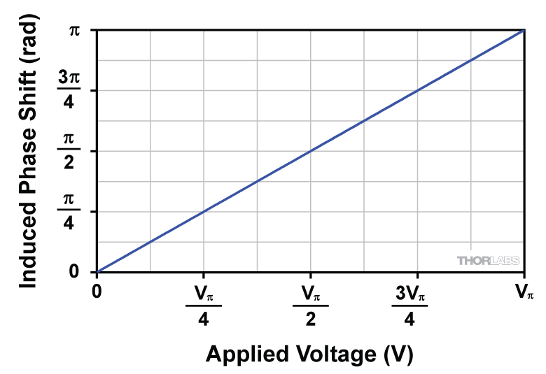
The most efficient LN phase modulators (PMs) use input light that is vertically polarized along the same crystal axis as the applied voltage (z-axis), as shown in Figure 2a. Because the light is linearly polarized along only one of the principal birefringent axes, the SPR does not play a role, and the output polarization remains vertically polarized. In many applications, the absolute phase delay resulting from propagation at the output of the modulator is irrelevant. Only the modulated phase shift due to an applied voltage matters.
The applied modulation voltage, V(t), modulates nz , changing the optical path length and hence the phase shift of the output light. The half-wave voltage, known as Vpi, denotes the modulation voltage required to induce a pi (180°) phase shift. Figure 2b shows the voltage-induced phase shift due to the applied V(t). Here one can see that the resultant phase shift of the output light is linearly proportional to the applied voltage. The actual value of Vpi is a function of many factors (e.g. crystal dimensions and wavelength of light). For standard Thorlabs PMs, Vpi at 633 nm is about 150 V.
Click to Enlarge
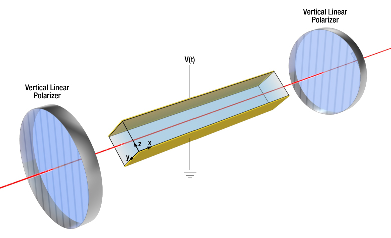
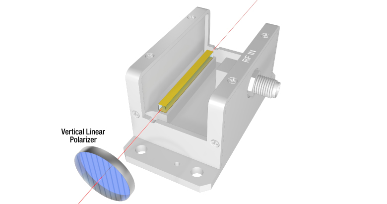
Figure 3: Schematic of the Polarization Modulator Configuration
EO Polarization Modulator
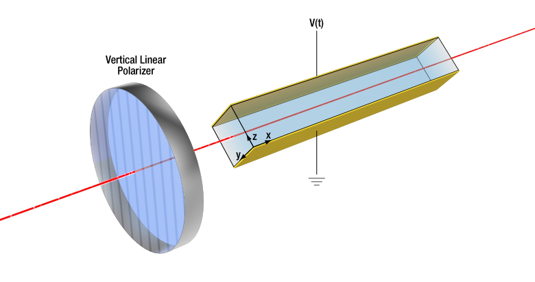
In an amplitude modulator (AM), the crystal is rotated 45° with respect to the modulator housing, while the input polarizer remains vertically oriented. Figure 3 illustrates this configuration. This results in the input light being equally split into two linear polarizations along the crystal y-axis and z-axis. These two components then develop a phase difference as they propagate through the crystal. This is the same principle as the SPR that was introduced earlier. We will now see that an applied voltage can introduce additional phase retardance, which we will call the voltage-induced phase retardance (VPR).
The applied voltage, V(t), changes the refractive indices along both the y-axis and z-axis, which introduces additional change to the phase retardance of the crystal. This additional voltage-induced phase retardance is called the VPR, which contributes to the total phase retardance (TPR) as given by:
TPR = SPR + VPR
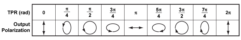
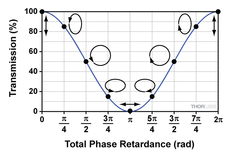
It is the TPR that now determines the net phase retardance of the crystal. For example, in this case, when the TPR equals pi, the crystal behaves like a half-wave plate, resulting in a horizontal linear output polarization. A TPR of pi/2 would convert the linearly polarized input into a circularly polarized output, like a quarter-wave plate. Other phase differences yield various elliptical polarization states. In this way, the LN crystal rotated at 45° functions as a polarization modulator, as shown for a few standard cases in Figure 4.
Click to Enlarge
Figure 4: Above is the relationship between the output polarization state and the total phase retardance imparted by the crystal, assuming the input polarization is vertical.
Click to Enlarge
Figure 5b: Ideal Amplitude Modulator Transmission Function with Parallel Polarizers
Click to Enlarge
Figure 5a: Schematic of the Amplitude Modulator Configuration with Parallel Polarizers
Click to Enlarge
Figure 6b: Ideal Amplitude Modulator Transmission Function with Crossed Polarizers

Click to Enlarge
Figure 6a: Schematic of the Amplitude Modulator Configuration with Crossed Polarizers
EO Amplitude Modulator
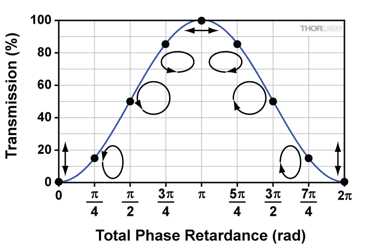
To create an amplitude modulator, a linear polarizer is placed at the crystal output to convert polarization change into amplitude change. Figure 5a depicts one configuration, where the second polarizer is oriented parallel to the first. The fraction of light transmitted through the output polarizer depends on the polarization of the light exiting the crystal. Only the polarization component aligned with the polarizer is transmitted. The transmission function, as shown in Figure 5b, is given by:
T = cos2(TPR/2)
where, as in the previous section, TPR = SPR + VPR.
For amplitude modulators, Vpi refers to the voltage required to induce a VPR of pi (or 180°). If the TPR = 0, then polarization does not change from input to output, and the output polarizer permits maximum transmission. When TPR = pi, the output polarization changes to horizontal, giving minimum transmission through the vertical polarizer. If the TPR is further adjusted to equal 2pi (or 360°), the transmission is once again maximized. It is important to note the cos2 transmission function is periodic, so the transmission is the same for all multiples of 2pi.
Note that if the output polarizer is changed to horizontal (or more generally, crossed relative to the input polarizer), as shown in Figure 6a, then the curve in Figure 5b would shift along the horizontal axis by pi. This results in the transmission function shown in Figure 6b, where maximum transmission is now at a TPR = pi.
Click to Enlarge
Figure 7: The above graph shows the effect of an arbitrary SPR on the voltage transmission response.
Effect of SPR in Amplitude Modulators
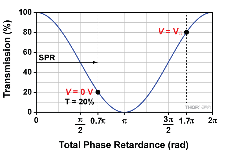
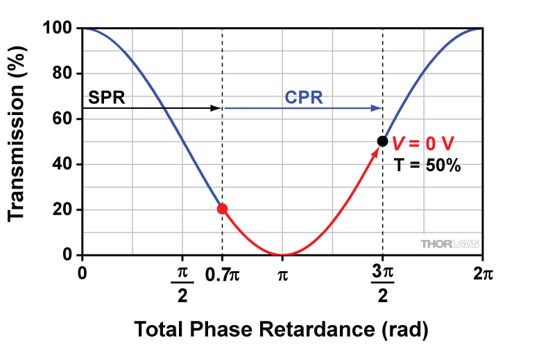
In practice, due to the unpredictable value of the SPR (which can be anything between 0 and 2pi), the transmission maximum likely does not occur at V = 0 V. SPR is a function of many factors like wavelength, temperature, and precise crystal dimensions. Out of the box, your EO modulator will probably have a nonzero SPR, meaning the transmission may take any value from 0 to 100% when V = 0 V (neglecting any losses from reflection and absorption).
The transmission curve in Figure 7 shows the effect of the SPR. For the sake of this example, we set the SPR at an arbitrary 0.7pi, but note that your modulator’s SPR can be anywhere between 0 and 2pi. In this example, the 0.7pi SPR sets the operating point (V = 0 V) transmission at ≈20%. Consequently, an applied voltage of Vpi would add an additional pi of VPR and thus give ≈80% relative transmission. Given the 0.7pi SPR in this example, you would have to add a voltage that induces an additional VPR of 0.3pi to reach the first transmission minimum. Or if you wanted to reach the maximum transmission, you would have to add a voltage that induces an additional 1.3pi of VPR.
Click to Enlarge
Figure 8: The above graph shows the effect of an arbitrary SPR on the voltage transmission response. CPR is added to SPR to set a new V = 0 V operating point.
Amplitude Modulator Compensation
The SPR results in an arbitrary transmission at 0 V, yet many applications require the modulator to be set at a specific transmission point like peak (T = 100%), quadrature (T = 50%), or null (T = 0%). In such cases, we must compensate for the SPR to reach the desired operating point. This is done by adding a compensating phase retardance, CPR. Methods for adding CPR are described in the next section. There are then three components to the TPR:
TPR = SPR + VPR + CPR
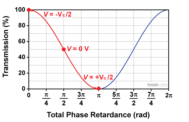
Figure 8 shows the transmission function and the same arbitrary, nonzero SPR used in the previous section. In this example, we add 0.8pi of compensation to reach the quadrature operating point (i.e., TPR = 3pi/2 and T = 50% at V = 0 V). Note you can add or subtract any value of compensation to reach any desired operating point.
It should also be noted that it is often possible to create custom versions of the modulator for specific wavelength applications that do not require an adjustable compensator. Please contact Thorlabs' Tech Support to discuss this.
Click to Enlarge
Figure 10: Amplitude Modulator Transmission Function at a Quadrature Operating Point

Click to Enlarge
Figure 9: Schematic of the Amplitude Modulator with Optical Compensation
Compensation Methods
If compensation is necessary to set a specific operating point for your application, then one of two main compensation methods can be employed: electrical or optical. The first method simply uses an applied DC voltage, VDC, in addition to the applied modulation voltage. In the example given in Figure 8, one must add a DC voltage of 0.8Vpi to reach the 50% transmission point. The equation for CPR then looks like this:
CPR = pi ⋅ VDC / Vpi = 0.8pi
The static DC voltage introduces an electrically tunable component to the CPR. This electrical DC compensation scheme works well at most wavelengths, but it’s worth noting that light at shorter wavelengths (400 - 600 nm) can actually produce an internal electric field that negates the applied DC electric fields.
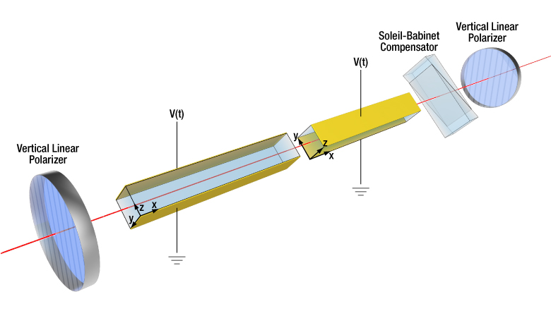
The second method, optical compensation, however, works uniformly well at all wavelengths. For this we typically use a tunable waveplate, such as a Soleil-Babinet compensator. As shown in Figure 9, when aligned with the crystal's axes, the compensator introduces an optically tunable CPR. This is especially advantageous in the case of non-resonant amplitude modulators at long wavelengths, where extremely high voltages would be required for pure electrical compensation.
One of the benefits of optical compensation is that it can reduce the absolute voltage required for full modulation. In the AM example, setting the operating point at peak (T = 100%) or null (T = 0%) requires the full Vpi voltage to swing between a transmission minimum and a maximum. Alternatively, when the operating point is set to quadrature (T = 50%), the required voltage range becomes -Vpi/2 to +Vpi/2. This means the absolute value of the drive voltage is effectively cut in half, but it does need to be a bipolar source to allow both the addition and subtraction of VPR, as shown in Figure 10.
Click to Enlarge
Figure 11: Schematic of the Temperature-Compensated Amplitude Modulator with Optical Compensation
Temperature-Independent Amplitude Modulator
One of the tricky issues with LN modulators is that the crystal’s refractive indices are temperature-dependent due to the thermo-optic effect. To prevent the output polarization state from drifting with temperature, our amplitude modulators contain a second, matched crystal that is rotated by 90° with respect to the first. Figure 11 depicts this configuration. (Note: Thorlabs' PMs contain a single 40 mm long crystal, while AMs contain two 20 mm long crystals).
Each crystal independently contributes to the SPR, as given by:
TPR = SPR1 + SPR2 + VPR + CPR
where SPR1 and SPR2 are the static phase retardances introduced by the first and second crystals, respectively. Because the second crystal is rotated by 90°, its birefringent axes (y and z) are also rotated. Therefore, the SPR of the second crystal compensates for the SPR of the first. If the crystal lengths are perfectly matched, then SPR1 = -SPR2, and
TPR = VPR + CPR
In this way, the matched crystals compensate the thermal fluctuations in SPR, giving the modulator a temperature sensitivity below 0.01 rad/°C (in units of SPR per °Celsius). The matched crystals do not affect the modulation efficiency because they do not compensate the VPR, only the SPR. However, due to manufacturing constraints, there will still be some residual SPR. Even a small, μm-scale mismatch in crystal length can give an SPR anywhere from 0 to 2pi. Though the matched crystal pair gives effective thermal compensation, you will still need to use one of the compensation methods described in the previous section to set your operating point.
Click to Enlarge
Figure 12b: Orientation of the Polarizers with Respect to the EO Modulator Housing for an Amplitude Modulator
Click to Enlarge
Figure 12a: Orientation of the Polarizer with Respect to the EO Modulator Housing for a Phase Modulator
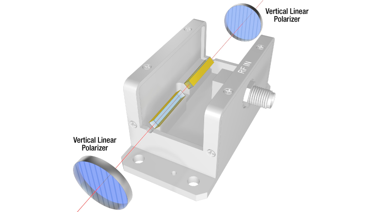
Operation in the Thorlabs Housing
Figures 12a and 12b show the orientation of the LN crystals and linear polarizers with respect to the modulator housing. The EO modulators contain only an LN crystal (two for amplitude modulators) and the electronic circuit to apply the external drive voltage. They do not contain the linear polarizers or optical compensator depicted in the previous sections. Phase modulators require only an input polarizer with vertical orientation (or a polarized laser source), while amplitude modulators require both input and output polarizers.
Figure 12a depicts the standard phase modulator (PM), while Figure 12b shows the configuration of the amplitude modulator (AM). The PM crystal is the same length as two AM crystals, so the half-wave voltages for either model are similar for a given wavelength. To be more precise, PMs always have a lower Vpi than the AM equivalent because the single polarization of the phase modulator sees a higher effective EO coefficient than the net EO coefficient between two orthogonal polarizations in the amplitude modulator.
Note that the input polarizer is not needed for either version of the modulator if the laser source is already vertically linear polarized. It is also possible to run these modulators with alternate polarization schemes, but that is beyond the scope of this document. Please contact Thorlabs' Tech Support for more information.
Driving EO Modulators
Driving free-space modulators can sometimes be challenging. Our HVA200 high-voltage amplifier, which features a low-noise, ±200 V output and 1 MHz bandwidth, is ideal for driving our broadband, non-resonant EO modulators when certain operating conditions are met. The 400 V output swing allows the HVA200 to fully modulate our non-resonant AMs for wavelengths up to ~1200 nm and our non-resonant PMs across all wavelengths. The HVA200 also provides an adjustable DC bias to allow for electrical compensation to the quadrature operating point of an amplitude modulator, and effectively utilize the ±200 V bipolar output swing.
For driving non-resonant modulators at frequencies higher than 1 MHz, or at longer wavelengths, specialized amplifiers with sufficient output power, linearity, and bandwidth are required. Additionally, for non-resonant modulators, the driver should be able to drive a purely capacitive load. These devices do not present with a standard 50 Ω input impedance.
Thorlabs also provides resonant modulators that have reduced input voltage requirements. These modulators (both AM and PM) come with an internal circuit that resonates at a specific frequency. This effectively multiplies the amplitude of the external sinusoidal drive signal to the higher voltage levels the EO crystals require. The trade-off is that these modulators only operate at a specific design frequency between 1 MHz and 100 MHz. Resonant modulators that operate at 20 MHz are available from stock, but other frequencies can be requested.
Please see the full web presentation for more details about resonant and non-resonant modulators, and contact Tech Support for any more specific information or custom requests.
| Posted Comments: | |
| No Comments Posted |