Auto-Balanced Detector with Avalanche Photodiodes

- Designed for Low-Power Applications Between 1200 and 1700 nm
- DC - 400 MHz Bandwidth
- >35 dB Common Mode Rejection Ratio (Typical)
- Fiber-Coupled FC/APC Inputs
PDB570C
Right View of
PDB570C
SMA Connectors
for Output Signal
Input for
Power Cord

Please Wait
| Balanced Detector Selection Guide |
|---|
| Balanced Detectors with Fast Monitor Output |
| Large-Area Balanced Amplified Detectors |
| Suitable for OCT |
| Compact Balanced Amplified Detectors |
| Compact Balanced Detectors |
| OCT Balanced Detectors with Fast Monitor Output |
| Auto-Balanced Detector with Avalanche Photodiodes |
| Polarization-Dependent Balanced Detector |
| Selected Specificationsa | |
|---|---|
| Operating Wavelength Range | 1200 - 1700 nm (Optimized for 1300 nm) |
| Typical Responsivityb | 0.9 A/W @ 1300 nm |
| Bandwidth (3 dB; Balanced/Auto-Balanced) |
DC to 400 MHz |
| Min NEP (DC to 100 MHz)c | 1.0 pW/√Hz |
| Common Mode Rejection Ratio | >25 dB (>35 dB Typical) |
| Transimpedance Gain, High Zd | 2 x 10³ V/A |
| Detector Type | InGaAs APD |
| Internal Coupling Fiber | SMF-28e+ |
| Optical Inputs | FC/APC |
Features
- Optical Gain Control and Auto-Balance Function
- Avalanche Photodiodes (APDs) Excellent for Low-Input-Power Applications
- Optimized for 1300 nm
- Operating Wavelength Range: 1200 - 1700 nm
- Wide DC to 400 MHz Bandwidth
- Exceptionally Low NEP: 1.0 pW/√Hz (DC - 100 MHz)
- >35 dB Common Mode Rejection Ratio (Typical)
- <0.4 mVRMS Output Voltage Noise
- Fiber-Coupled FC/APC Inputs
- Switchable Universal Power Supply Included
Thorlabs' PDB570C Avalanche-Photodiode-Based Balanced Detector is a balanced receiver that subtracts the two input signals from each other, resulting in the cancellation of common mode noise. The balanced detector, which uses two well-matched avalanche photodiodes (APDs) and an ultra-low-noise, ultra-low-distortion, high-speed transimpedance amplifier, is optimized for applications with low optical input powers (minimum NEP of 1.0 pW/√Hz). Each avalanche photodiode is fiber coupled to the FC/APC outputs via length-matched SMF-28e+ fibers so as not to introduce optical path differences between the input and the active area of the photodiode. Compared to our other balanced detectors that use Si or InGaAs PIN photodiodes, the PDB570C offers unique features such as exceptionally low NEP, optical gain control, and an auto-balancing function with a variable closed-loop control velocity.

Click to Enlarge
The mating sleeve can be removed to access the FC/APC ferrules for cleaning.
This balanced detector features an adjustable gain and three different detection modes: single detector, balanced (BAL), and auto-balanced (AUTO-BAL). The single detector mode allows the output of each photodiode to be measured individually. In the BAL mode, the PDB570C functions as a standard balanced detector while allowing the optical gain of both photodiodes to be simultaneously adjusted. In the AUTO-BAL mode, the balanced detector compensates for power differences between the two optical input signals that vary at a slower rate than a cutoff frequency set via the CONTROL VELOCITY knob. This power difference can be monitored via the CONTROL OUTPUT and will not contribute to the voltage generated by the balanced detector at the RF output. For details on how to operate the PDB570C, please see the Detector Operation tab.
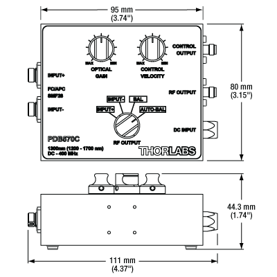
The included post-mounting adapter plate has both 8-32 and M4 taps and can be attached to either the bottom or back of the PDB570C's shielded aluminum housing with the included M2 x 8 screws. The PDB570C's compact housing is 95 mm x 80 mm x 44.3 mm (3.74" x 3.15" x 1.74"), including the depth of the control knobs. Each detector is shipped with a ±12 V DC power supply with an input voltage of 115 V or 230 V that can be selected by a switch. A replacement power supply that supports input voltages of 100, 120, and 230 V is available below.
The exceptionally low noise of the PDB570C APD-based auto-balanced detector makes it suitable for OCT applications. The full range of our PIN photodiode-based balanced detectors that can be used for OCT applications are found here. Thorlabs also offers Fiber-Based Interferometers, which feature an integrated balanced detector.
While the PDB570C is intended for fiber-coupled applications, a free-space beam can be coupled into the FC/APC inputs via a pigtailed aspheric collimator. Care should be taken to length-match the fibers between the collimator and the inputs in an attempt to avoid introducing unwanted path length differences into the system. Thorlabs also offers balanced detectors designed for free-space applications. Additionally, some of our fiber-coupled balanced detectors with fast monitor outputs have removable FC/APC detectors for easy integration into free-space applications.
| Specifications | |
|---|---|
| Detector | |
| Detector Type | InGaAs APD |
| Optical Inputs | FC/APC |
| Internal Coupling Fiber | SMF-28e+ |
| Coupling Loss | <0.5 dB (<0.3 dB Typical) |
| Operating Wavelength | Optimized for 1300 nm (1200 to 1700 nm Operating Range) |
| Max Responsivity (Typical)a | 0.9 A/W @ 1300 nm |
| Optical Back Reflection (at the Detector Surface) | <-40 dB |
| Max Input Power (Damage Threshold)b | 200 µW |
| RF Output | |
| Bandwidth (3 dB; Balanced/Auto-Balanced) | DC to 400 MHz |
| Bandwidth (3 dB; INPUT+/INPUT -) | DC to 300 MHz |
| Common Mode Rejection Ratio | >25 dB (>35 dB Typical) |
| Transimpedance Gain, High Zc | 2 x 10³ V/A |
| Optical Gain Factor | 2.5 to 10, Adjustable |
| Conversion Gain at 1300 nmc | 4.5 x 10³ to 18.0 x 10³ V/W |
| CW Saturation Powerb | 200 µW @ 1300 nm |
| RF Output Coupling | DC Coupling Only |
| RF Output Impedance | 50 Ω |
| Max RF OUTPUT Voltage Swing | ±4.2 V (High Z Load) ±2.1 V (50 Ω Load) |
| Min NEP (DC to 100 MHz)b,d | 1.0 pW/√Hz |
| Overall Output Voltage Noise | <0.4 mVRMS |
| Typical DC Offset | ±3 mV |
| Control Output | |
| Impedance | 1 kΩ |
| Voltage Swing, High Z Load | ±4.7 V (Max) |
| General | |
| Electrical Outputs | SMA |
| Included Power Supplye | ±12 V @ 250 mA (100/120/230 VAC, 50 - 60 Hz, Switchable) |
| Operating Temperature Range (Non-Condensing) | 0 to 40 °C |
| Storage Temperature Range | -40 to 70 °C |
| Dimensions without Connectors (W x H x D)f | 95 mm x 80 mm x 44.3 mm (3.74" x 3.15" x 1.74") |
| Weight | 0.37 kg (0.82 lbs) |
Click to Enlarge
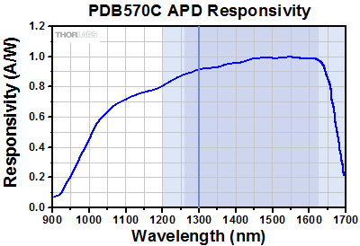
The blue-shaded regions indicate the specified 1200 - 1700 nm operating wavelength range of the PDB570C APD balanced detector. Optimal performance is obtained for wavelengths between 1260 nm and 1625 nm, which is denoted by the darker blue shaded region; this optimized region is narrower due to the optical properties of the SMF-28e+ fiber used to couple the photodiodes to the inputs. The fiber pigtails may introduce additional insertion loss outside of this range and transmit multi-modal light below the fiber's 1240 nm cutoff wavelength. The 900 to 1700 nm range of the graph indicates the full operating range of the APDs. This photodiode has been optimized for use at 1300 nm, which is indicated with a vertical blue line.
Click for Details
Simplified Mechanical Drawing of the PDB570C
Click to Enlarge
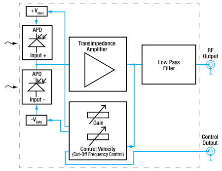
A functional diagram of the PDB570C. The transimpedance amplifier generates an output voltage proportional to the difference between the photocurrents of the two photodiodes. The gain of the detector and cut-off frequency for the auto-balance feature can be set by the user.
Thorlabs' PDB570C Balanced Detector with Avalanche Photodiodes features an adjustable gain and three different detection modes: single detector, balanced (BAL), and auto-balanced (AUTO-BAL). The single detector mode allows the output of each photodiode to be measured individually. In this mode, sources can be connected to both INPUT+ and INPUT-, while the RF OUTPUT knob can be used to select which input you wish to monitor. The optical gain control allows the RF OUTPUT signal level to be adjusted. This feature is helpful when setting your experiment to provide equal input power levels to each APD prior to continuing with measurements in the balanced or auto-balanced detection modes.
Click to Enlarge
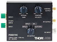
Front View of the PDB570C APD-Based Balanced Detector
In the BAL mode, the PDB570C functions as a standard balanced detector while allowing the optical gain of both photodiodes to be simultaneously adjusted. The output signal generated by the difference between the two input signals can then be measured via the RF OUTPUT connector.
In the AUTO-BAL mode, the optical gain control only affects INPUT-, while the gain for INPUT+ is automatically adjusted via a power-balance control loop to match the current generated by INPUT- (see the figure to the right). This circuit will compensate for power differences between the two optical input signals that vary at a slower rate than a cutoff frequency set via the CONTROL VELOCITY knob. Differences between the two input signals that vary slower than this frequency will not contribute to the voltage generated at RF OUTPUT. The CONTROL OUTPUT in auto-balance mode provides a measure of this rejected signal (i.e., the constant or slowly varying power imbalance between the two input optical signals). Therefore, the control circuit effectively functions as a lowpass filter for the CONTROL OUTPUT.
A second lowpass filter serves to remove noise from the output of the transimpedance amplifier before it is read out at RF OUTPUT. The CONTROL VELOCITY knob is not marked with graduated bandwidth values, as the control loop is affected by several factors including the optical gain, ratio of input power levels, absolute input power level, and the modulation depth of the disturbance signal.
Pin Diagrams for Auto-Balanced Detectors
Control Output
SMA Female
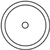
RF Output
SMA Female

PDB Male (Power Cables)
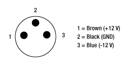
PDB Female (Photodetector)

| Posted Comments: | |
Nicola Coluccelli
(posted 2024-01-19 09:31:21.66) Dear Sirs,
I am working on frequency noise measurements of a laser at 2.1 micron. I would need an auto-balanced detector based on extended InGaAs photodiodes. Specifically, I would ask if it is possible to adapt the PDB570C electronics for use with extended InGaAs detector (model FD05D from Thorlabs). The bandwidth can be limited to 10 MHz, as I don't need to work at such a high frequency as the 400 MHz of the standard PDB570C. Could you provide this custom device? If so, can you please contact me by email for a quotation?
Regards,
Nicola Coluccelli fmortaheb
(posted 2024-01-19 09:58:22.0) Dear Nicola, Thank you very much for your inquiry. We will reach out to you directly to discuss your application. gilad zisman
(posted 2023-02-05 23:45:01.927) hi,
your data sheet does not give information regarding maximum input current.
can you please provide me this information.
thanks,
Gilad hkarpenko
(posted 2023-02-07 10:32:52.0) Dear customer,
thank you for your feedback. I´m reaching out to you directly, to discuss this issue in detail. Michael Slocum
(posted 2021-02-12 17:11:20.363) Following up on the comment from cbrideau, if you can't find a Si APD that can tolerate the high voltage bias, would it be possible to use a GaAs APD to achieve visible detection and the higher bandwidth? dpossin
(posted 2021-02-17 05:18:06.0) Dear Michael,
Thank you for your feedback. In general it is possible to offer APD in the VIS based on GaAs within our low voltage PCB design. I will reach out to you in order to discuss the technical details. hoju1301
(posted 2017-07-02 13:45:10.157) Hello! How does this perform compared to the Newport/New Focus Nirvana series auto balance detector? swick
(posted 2017-07-05 03:27:45.0) This is a response from Sebastian at Thorlabs. Thank you for the inquiry. I have contacted you directly for detailed comparison of the specifications. spiros.mikroulis
(posted 2016-09-23 09:20:02.27) I would like to have more info for the PDB570C.
First what can be the maximum input power level?
I see the max input power is 200 μW but can this be increased using low gain?
Spiros Mikroulis swick
(posted 2016-09-28 06:43:45.0) This is a response from Sebastian at Thorlabs. Thank you for the inquiry.
The optical damage threshold of PDB570C is 200µW. Applying optical power of more than 200µW to the PDB570C would result in damage. cbrideau
(posted 2015-01-16 15:12:38.04) Are there any plans to make these available with Si photodiodes like the APD120 or APD210 for use in the visible? This could be useful for a correlation project I have on the back burner for visible fluorescence. shallwig
(posted 2015-01-19 04:26:47.0) This is a response from Stefan at Thorlabs. Thank you very much for your inquiry. We are checking the market for APDs in the visible range which match with the layout of our PDB570C in terms of bias voltage. Unfortunately there are no APDs available which fit with our low voltage layout. The APDs which are available so far need about 150V while the InGaAs APDs only need 50V. We will go on checking the market for solutions and keep you informed. |

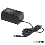
- Replacement Power Supply for the Balanced Amplified Photodetectors Sold Above
- ±12 VDC Power Output
- Current Limit Enabling Short Circuit and Overload Protection
- On/Off Switch with LED Indicator
- Switchable AC Input Voltage (100, 120, or 230 VAC)
- 2 m (6.6') Cable with LUMBERG RSMV3 Male Connector
- UL and CE Compliant
The LDS12B ±12 VDC Regulated Linear Power Supply is intended as a replacement for the supply included with our PDB line of balanced photodetectors sold on this page. The cord has three pins: one for ground, one for +12 V, and one for -12 V (see diagram to the right). A region-specific power cord is shipped with the unit based on your location. This power supply can also be used with the PDA series of amplified photodetectors, PMM series of photomultiplier modules, APD series of avalanche photodetectors, and the FSAC autocorrelator for femtosecond lasers.
 Products Home


 Zoom
Zoom
 Auto-Balanced Detector with Avalanche Photodiodes