Single-Crystal Diamonds

- Diamonds Grown by Chemical Vapor Deposition
- Quantum-Grade or Electronic-Grade Diamonds Available
- Uniform Distribution of NV Centers
ELSC45
NV: <0.03 ppb
4.5 mm x 4.5 mm x 0.5 mm
DNVB14
NV: 4.5 ppm
Coherence Time T2: 10 µs
3.0 mm x 3.0 mm x 0.5 mm
Application Idea
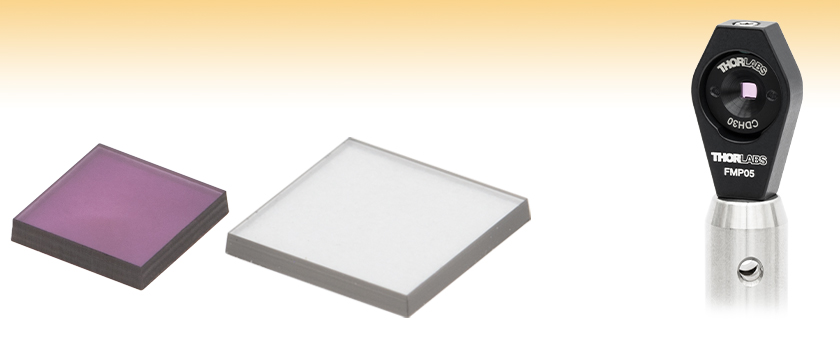
A DNVB14 3.0 mm square quantum-grade single-crystal diamond is mounted in an FMP05 Ø1/2" optics mount using a CDH30 square optics holder.

Please Wait

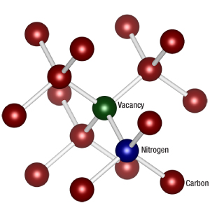
Figure 1.1 Nitrogen-vacancy (NV) centers are point defects where a nitrogen atom and adjacent vacancy replace a pair of carbon atoms in the diamond lattice.
Features
- Single-Crystal Diamonds Grown by Chemical Vapor Deposition (CVD)
- Quantum-Grade or Electronic-Grade Diamonds Available
- Nitrogen Vacancy Center Concentrations of <0.03 ppb, 300 ppb, and 4.5 ppm
These single-crystal diamonds, which are manufactured by Element Six using patented processes and offered by Thorlabs to enable quantum research advancements, are ideal for magnetic field sensing, RF detection, gyroscopes, masers, quantum demonstrations, quantum computing, quantum communication, and research applications. The quantum-grade diamonds are available with either 300 ppb or 4.5 ppm nitrogen-vacancy (NV) center densities. For users who wish to create their own defect centers, electronic-grade diamonds with <0.03 ppb NV concentration and low background impurity are available. These diamonds are useful for applications such as fabricating ionizing radiation-resistant devices.
For compatibility with Thorlabs' optomechanical components, we recommend mounting these single-crystal diamonds in our Ø1/2" adapters for unmounted square optics.

Click to Enlarge
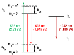
Figure 1.2 The energy level diagram for a diamond NV– center in zero magnetic field. The spin triplet ground (3A2) and excited (3E) states have an energy difference of 637 nm (1.945 eV), and each is split into singly degenerate ms = 0 and doubly degenerate ms = ±1 spin states with energy differences of Dgs = 2.88 GHz (12 µeV) and Des = 1.42 GHz (5.9 µeV), respectively. Note, the scale of the spin sub-level splitting is highly exaggerated to be visible. There are also two optically dark, ms = 0 intermediate states (1A and 1E) with an energy difference of 1042 nm (1.190 eV).

Click to Enlarge
Figure 1.3 The triplet ground state of an NV- center shows fine structure splitting (Dgs = 2.88 GHz) between the ms = 0 and ms = ±1 states due to spin-spin interactions. Application of an external magnetic field (B) along the [111] defect axis causes a further splitting (ΔE = 2gµBB) of the ms = ±1 states due to the Zeeman effect, where g is the Landé factor and µB is the Bohr magneton.

| Posted Comments: | |
David Dungey
(posted 2025-09-03 21:20:49.097) Hi, I'm a graduate student at Harvard and for my research project I need an NVC, I heard that TL has smaller/tiny samples of NVCs available? Is that true and how much would that cost? tdevkota
(posted 2025-09-04 01:26:57.0) Thank you for contacting Thorlabs. We do offer single-crystal diamonds with different nitrogen-vacancy (NV) center concentrations. You can find the dimensions, NV center density, pricing, availability, and other specifications for each optic on the product page. Jano Gil Lopez
(posted 2025-01-17 10:51:36.037) Dear Thorlabs team,
We would like to know if it is possible to experiment and test quantum memories with these products. We would need low density NV centers. Do you have any customers who have succesfully used them? Thank you.
Best regards,
Jano tdevkota
(posted 2025-01-21 04:52:07.0) Thank you for contacting Thorlabs. In principle, these materials can be used as a key element in a quantum memory setup. I have reached out to you directly to discuss your application further. Marcel van der Horst
(posted 2024-06-13 09:35:21.457) Dear sir, madam,
At the Amsterdam University of Applied Sciences, we want to develope our own NV-center magnetometers.
Can you please inform me how many diamonds are delivered when I buy "quantity 1" DNV B14 diamonds; is it one diamond or several diamonds in a package?
Thank you in advance for the information.
Best regards,
Dr. Marcel van der Horst
Amsterdam University of Applied Sciences/Sensor lab
Jakoba Mulderhuis, Rhijnspoorplein 2, 1091 GC Amsterdam
M: 06 2115 8862
http://www.hva.nl/opleiding/engineering-elektrotechniek/elektrotechniek.html?origin=euCvyOz3R2q5%2B5c%2BeyU0bQ jdelia
(posted 2024-06-13 12:34:04.0) Thank you for contacting Thorlabs. The DNVB14 consists of one diamond doped with NV-centers. Hassan TERMOS
(posted 2024-03-20 10:26:40.817) Dear Sir,
I would like to ask you if this type of crystal has fixed or variable grating periods.
The threshold power and maximum input power can depend on various factors, including crystal quality, pump wavelength, pump intensity, temperature control, and phase matching conditions. I already used a PPLN crystal; the threshold power was 4-6 W, while the maximum input pump power that crystal can afford is 20 W. The pump wavelength of the PS laser is 1064 nm.
Can I know the threshold power that indicates the minimum power required for efficient parametric generation to occur in the crystal and the maximum input pump power that represents the upper limit?
Best regards,
Hassan Termos jdelia
(posted 2024-04-04 12:55:25.0) Thank you for contacting Thorlabs. While PPPL has a periodicity associated with it, it does not really apply to diamond. Diamond is also not a traditional non-linear crystal so we can’t really suggest anything about pump lasers required. I have reached out to you directly to clarify your inquiry and discuss your application further. Benjamin Strycker
(posted 2023-10-04 16:18:30.397) For the NV diamond products, are the NV-axes oriented preferentially along the {111} direction, or are the NV-axes randomly oriented along the four crystallographic directions allowed in diamond? cdolbashian
(posted 2023-11-08 01:04:46.0) Thank you for reaching out to us with this inquiry. NVs will be randomly distributed amongst the four possible <111> directions with no preferred direction. Jing Zhou
(posted 2022-09-02 21:37:48.633) 您好,我想问一下关于:
1.DNVB1参数表里的Edge Features是什么意思?
2.NV色心在金刚石晶片表面均匀分布吗?
3.晶片中制作好的NV色心的深度(与上表面的距离)是多少? |

| Item # | DNVB1 | DNVB14 | |
|---|---|---|---|
| Quantum Properties | |||
| Typical NV Center Density | 300 ppb | 4.5 ppm | |
| Typical Spin Coherence Time T2* a | 1 µs | 0.5 µs | |
| Typical Spin Coherence Time T2 b | 200 µs | 10 µs | |
| General Specifications | |||
| Crystallographic (Face) Orientation | {100} ± 3° | ||
| Edge Orientation | <100> | ||
| Dimensionsc | Length | 3.0 +0.2/-0.0 mm | |
| Width | 3.0 +0.2/-0.0 mm | ||
| Thickness | 0.5 ± 0.05 mm | ||
| Laser Kerf | ≤5° | ||
| Edge Features | <0.2 mm | ||
| Roughness, Ra | <10 nm | ||
| 13C Fraction | 1.1% | ||
- Two NV Center Densities Available:
- DNVB1: 300 ppb
- DNVB14: 4.5 ppm
- Available as a 3.0 mm x 3.0 mm Square
These quantum-grade diamonds are available with either 300 ppb or 4.5 ppm nitrogen-vacancy (NV) center densities. This produces diamond NV (DNV) centers with readable and writable spin qubits that have long lifetimes at room temperature, advantages that arise from the structure and strong covalent bonds of diamond. The density of NV spin centers, their uniform distribution, the spin characteristics, and the compact form factor make this diamond ideal for magnetic field sensing, RF detection, gyroscopes, masers, quantum demonstrations, and research applications. The diamonds are offered as 3.0 mm x 3.0 mm squares and are compatible with Thorlabs' CDH30 adapter for unmounted square optics.
Please note that to avoid damage, these diamonds should be handled using non-metallic tools like the TZ1 Carbon-Fiber Tipped Tweezers.

| Item # | ELSC20 | ELSC40 | ELSC45 | |
|---|---|---|---|---|
| Crystallographic (Face) Orientation | {100} ± 3° | |||
| Edge Orientation | <110> | |||
| Dimensionsa | Length | 2.0 +0.2/-0.0 mm | 4.0 +0.2/-0.0 mm | 4.5 +0.2/-0.0 mm |
| Width | 2.0 +0.2/-0.0 mm | 4.0 +0.2/-0.0 mm | 4.5 +0.2/-0.0 mm | |
| Thickness | 0.5 ± 0.05 mm | |||
| Laser Kerf | <5° | |||
| Edge Features | <0.2 mm | |||
| Roughness, Ra | <5 nm | |||
| Boron Concentration | <1 ppb | |||
| Nitrogen Concentration | <5 ppb | |||
| Typical NV Concentration | <0.03 ppb | |||
| 13C Fraction | 1.1% | |||
- Low Nitrogen-Vacancy (NV) Center Density: <0.03 ppb
- Available in Three Sizes:
- 2.0 mm x 2.0 mm Square
- 4.0 mm x 4.0 mm Square
- 4.5 mm x 4.5 mm Square
These electronic-grade, single-crystal diamonds contain <5 ppb nitrogen concentration and typically <0.03 ppb nitrogen-vacancy (NV) concentration. Additionally, the diamonds have a very low background impurity of <1 ppb boron concentration and exhibit electron mobility from 1000 - 1700 cm2/V⋅s. These diamonds allow the user to probe the as-grown NV defects or generate their own via ion implantation or epitaxial growth. Alternatively, they can be used as a high thermal conductivity and optically transparent heat sink for a high power laser or microelectronic device, as well as for custom-made diamond electronic devices such as radiation detectors. The diamonds are offered as 2.0 mm x 2.0 mm, 4.0 mm x 4.0 mm, or 4.5 mm x 4.5 mm squares and are compatible with Thorlabs' Ø1/2" adapters for unmounted square optics.
Please note that to avoid damage, these diamonds should be handled using non-metallic tools like the TZ1 Carbon-Fiber Tipped Tweezers.
 Products Home


 Zoom
Zoom
 Diamonds with Nitrogen-Vacancy Centers