Free-Space Biased Detectors
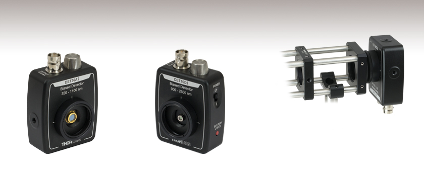
- Monitor CW or Fast Pulsed Lasers
- Detectors for Wavelengths from 200 to 2600 nm
- Integrate with Cage or Lens Tube Systems
DET36A2
Biased Si Detector
Application Idea
DET Series Detector Attached to a 30 mm Cage System Using the Included SM1 Coupler and an SM1T2 Adapter
(See the Housing Tab for Details)
DET10D2
Biased InGaAs Detector

Please Wait
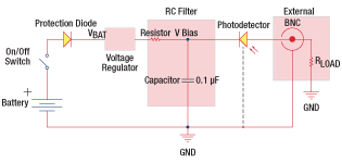
Operating Circuit Diagram
Click to Enlarge
The detectors are reverse biased to produce a linear response with applied input light.
Click to Enlarge
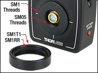
Each detector has an internal SM05 and external SM1 thread and comes with an
attached SM1T1 Internal SM1 Adapter
and SM1RR Retaining Ring.
Features
- Models Covering the 200 nm to 2.6 μm Wavelength Range
- Rise Times as Fast as 1 ns
- Compact Housing for Measurements in Tight Spaces
- SM05 Lens Tube, SM1 Lens Tube, Cage System, and Ø1/2" Post Compatible
- Internal A23 12 V Bias Battery Included
- Optional Power Adapter and Power Supply Available Below
- Can be Fiber Coupled Using Our Internally and Externally SM1-Threaded Fiber Adapters
Thorlabs' Biased Photodetectors are available in models that cover the wavelength range from the UV to the mid-IR (200 nm to 2.6 µm). The slim housing allows the optical detector to slip into tight setups. Our Si and InGaAs detectors are based on fast PIN photodiodes, whereas our Ge detectors are based on N-on-P type photodiodes. Every detector comes complete with an internal bias battery packaged in a rugged aluminum housing. Our biased photodetectors are compatible with our benchtop photodiode amplifier and PMT transimpedance amplifier.
With a wide bandwidth DC-coupled output, these detectors are ideal for monitoring fast pulsed lasers as well as DC optical sources. The direct photodiode anode current is provided on a side panel BNC. This output is easily converted to a positive voltage using a terminating resistor. When looking at high-speed signals, Thorlabs recommends using a 50 Ω load resistor. For lower bandwidth applications, our variable terminator or fixed stub-style terminators quickly adjusts the measured voltage. The detectors below do not have amplifiers or built-in gain, which generally allows them to operate at higher speeds than our PDA series of amplified photodetectors; for applications that require gain or switchable filters, a PDA amplified photodetector may be more suitable.
Click to Enlarge
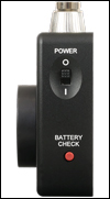
The Red Battery Test Button on the DET10D2
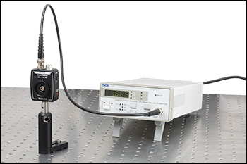
Click to Enlarge
PDA200C Benchtop Photodiode Amplifier Connected to a DET10A2 Photodetector Using a BNC Cable
All connections and controls are located away from the light path, which simplifies integration of our detectors in enclosed spaces. Every detector has internal SM05 (0.535"-40) threading and external SM1 (1.035"-40) threading. Each DET housing includes a detachable Ø1" Optic Mount (Item # SM1T1) that allows for Ø1" optical components, such as optical filters and lenses, to be mounted along the optical axis. Each DET detector can also be mounted in a cage system, lens tube system, or on a Ø1/2" optical post. Every unit's housing features two universal mounting holes that accept both 8-32 and M4 threads. For more information about the location of these mounting points and mounting these units, please see the Housing Features and Mounting Options tabs.
Each detector is reverse-biased by an A23 12 VDC battery incorporated into the housing. The housing also includes a red button (pictured to the left) which, when held down, applies the battery's voltage across the external load. For a high-Z load, this will output the battery's voltage over BNC, providing an easy way to determine if the battery should be replaced without removing it from the housing. An in-line current-limiting resistor prevents fast battery drainage if the battery is tested while connected to a 50 Ω load. Please note that due to slight physical variations of the positive terminal from manufacturer to manufacturer, Thorlabs only recommends using an Energizer® battery in our DET series of photodetectors. A battery was chosen for the reverse bias because it provides an extremely low noise source of power. If the finite lifetime of a battery is not acceptable, the battery can be replaced by a DET2B power adapter bundle. Extra batteries and the DET2B are available for purchase below.
Please note that inhomogeneities at the edges of the active area of the detector can generate unwanted capacitance and resistance effects that distort the time-domain response of the photodiode output. Thorlabs therefore recommends that the incident light on the photodiode is well centered on the active area. The SM1 (1.035"-40) threading on the housing is ideally suited for mounting a Ø1" focusing lens or pinhole in front of the detector element.
Thorlabs also offers high-speed free-space detectors and high-speed fiber-coupled detectors for wavelengths between 400 - 1700 nm.

Click to Enlarge
All detector housings have a red battery check button. The DET10D2 is shown here.

Click to Enlarge
Each detector has an internal SM05 and external SM1 thread and comes with an
attached SM1T1 Internal SM1 Adapter
and SM1RR Retaining Ring.
DET Series Housing Features
Thorlabs' high-speed detectors feature a slim design. Each housing features internal SM05 (0.535"-40) threading and external SM1 (1.035"-40) threading. Each detector includes an SM1T1 internally SM1-threaded adapter and an SM1RR retaining ring, as shown to the right. The SM1T1 can hold up to 0.1" (2.8 mm) thick optics. The detectors can be mounted using a 1/2" Post, as shown in the images below. Every detector has a housing design that features the active area flush with the front of the housing, simplifying alignments within optomechanical systems. This design also has two universal mounting holes that accept both 8-32 and M4 threads. As a convenience, the back panel is engraved with the responsivity curve of the photodiode.
Lens Tube Compatibility
These detectors can be integrated into various optomechanical systems using the internal SM05 and external SM1 threads. A lens tube can be directly attached to the SM1 threads, making the detectors compatible with lens tube systems. The SM1T1 adapter can be used to mount Ø1" (Ø25.4 mm) optical components, such as optical filters and lenses.
Cage System Compatibility
The detectors are also cage system compatible, as shown in the two images below right. A CP33(/M) cage plate can be attached directly to the SM1 threads. This attachment method does not require an adapter piece and allows the diode to be as close as possible to the cage plate, which can be important in setups where the light is divergent. Another method for integrating a detector into a cage system is using the included SM1T1 with an SM1T2 adapter. This allows more freedom in choosing the orientation of the detector. Additionally, these detectors can be used with SM1-threaded fiber adapters (sold below).
Post Mounting
Threaded holes on the housings of the detectors allow the units to be mounted in a horizontal or vertical orientation using a 1/2" Post. This gives the user the option to route the BNC cable from above or alongside the beam path, as shown below left.
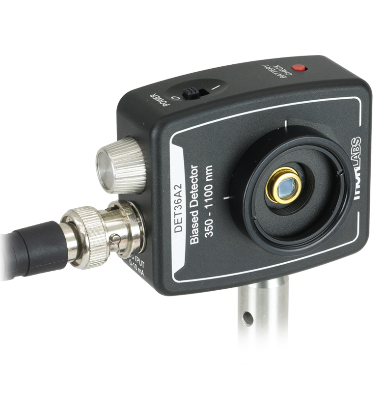
Click to Enlarge
DET Photodetector Mounted Horizontally
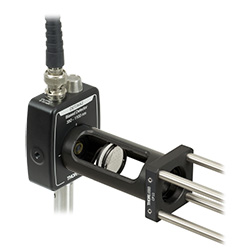
Click to Enlarge
DET Photodetector Connected to an SM1 Lens Tube in a 30 mm Cage System
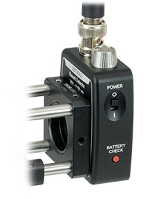
Click to Enlarge
DET Photodetector Integrated into a 30 mm Cage System Using the External SM1 Threads
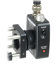
Click to Enlarge
DET Photodetector Integrated into a 30 mm Cage System Using the SM1T1 (included) and SM1T2 Adapter
Output Signal (Photocurrent)
BNC Female
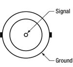
We recommend installing a 50 Ω terminating resistor (e.g., Item # T4119) to the BNC output of each detector. For max photocurrent output, please see the Housing Features column in the tables below.
Note: Our previous generation of free-space biased detectors specified an output voltage, which provided information about the max voltage output under the saturation limit, but the output signal was a photocurrent. To avoid confusion, our current generation of detectors now specify the output current. We apologize for any inconvenience this may have caused.
Battery Lifetime
When using a battery-operated photodetector, it is important to understand the battery’s lifetime and how this affects the operation of the detector. As a current output device, the output current of the photodetector is directly proportional to the amount of incident light on the detector. Most users will convert this current to a voltage by using a terminating load resistor. The resistance value is approximately equal to the circuit gain. For very high speed detectors, such as the DET08 series, it is very important to use a 50 Ω terminating resistor to match the impedance of standard coaxial cables to reduce cable reflections and improve overall signal performance and integrity. Most high-bandwidth scopes come equipped with this termination.
The battery usage lifetime directly correlates to the current used by the detector. Most battery manufacturers provide a battery lifetime in terms of mAh (milliamp hours). For example, if a battery is rated for 190 mA hrs, it will reliably operate for 190 hr at a current draw of 1.0 mA. This battery will be used in the following example on how to determine battery lifetime based on usage.
For this example we have a 780 nm light source with an average 1 mW power is applied to a detector. The responsivity of a biased photodetector based on the response curve at this wavelength is 0.5 A/W. The photocurrent can be calculated as:
![]()
Given the battery has a rated lifetime of 190 mA hr, the battery will last:

or 16 days of continuous use. By reducing the average incident power of the light to 10 µW, the same battery would last for about 4 years when used continuously. When using the recommended 50 Ω terminating load, the 0.5 mA photocurrent will be converted into a voltage of:

If the incident power level is reduced to 40 µW, the output voltage becomes 1 mV. For some measurement devices this signal level may be too low and a compromise between battery life and measurement accuracy will need to be made.
When using a battery-powered, biased photodetector, it is desirable to use as low a light intensity as is possible, keeping in mind the minimum voltage levels required. It is also important to remember that a battery will not immediately cease producing a current as it nears the end of its lifetime. Instead, the voltage of the battery will drop, and the electric potential being applied to the photodiode will decrease. This in turn will increase the response time of the detector and lower its bandwidth. As a result, it is important to make sure the battery has sufficient voltage (as given in the Troubleshooting chapter of the detector's manual) for the detector to operate within its specified parameters. The voltage can be checked with a multimeter.
Another suggestion to increase the battery lifetime is to remove, or power down the light source illuminating the sensor. Without the light source, the photodetector will continue to draw current proportional to the photodetector’s dark current, but this current will be significantly smaller.
For applications where a DET series photodetector is continuously illuminated with a relatively high-power light source, or if having to change the battery is not acceptable, we offer the DET2B power adapter bundle, which includes the power adapter and power supply (sold below). The drawback to this option is the noise in the line voltage will add to the noise in the output signal and could cause more measurement uncertainty.
Photodiode Tutorial
Theory of Operation
A junction photodiode is an intrinsic device that behaves similarly to an ordinary signal diode, but it generates a photocurrent when light is absorbed in the depleted region of the junction semiconductor. A photodiode is a fast, highly linear device that exhibits high quantum efficiency and may be used in a variety of different applications.
It is necessary to be able to correctly determine the level of the output current to expect and the responsivity based upon the incident light. Depicted in Figure 1 is a junction photodiode model with basic discrete components to help visualize the main characteristics and gain a better understanding of the operation of Thorlabs' photodiodes.

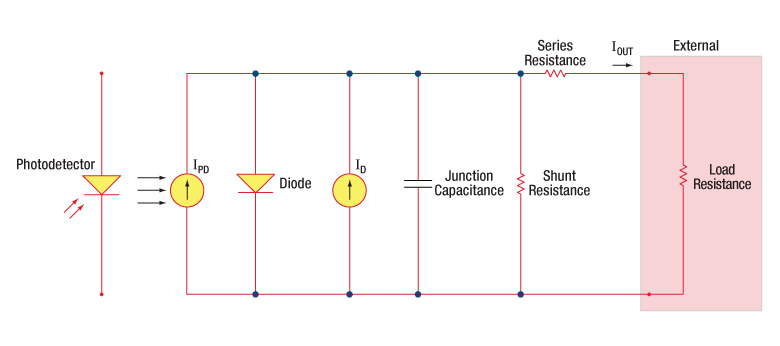
Figure 1: Photodiode Model
Photodiode Terminology
Responsivity
The responsivity of a photodiode can be defined as a ratio of generated photocurrent (IPD) to the incident light power (P) at a given wavelength:

Modes of Operation (Photoconductive vs. Photovoltaic)
A photodiode can be operated in one of two modes: photoconductive (reverse bias) or photovoltaic (zero-bias). Mode selection depends upon the application's speed requirements and the amount of tolerable dark current (leakage current).
Photoconductive
In photoconductive mode, an external reverse bias is applied, which is the basis for our DET series detectors. The current measured through the circuit indicates illumination of the device; the measured output current is linearly proportional to the input optical power. Applying a reverse bias increases the width of the depletion junction producing an increased responsivity with a decrease in junction capacitance and produces a very linear response. Operating under these conditions does tend to produce a larger dark current, but this can be limited based upon the photodiode material. (Note: Our DET detectors are reverse biased and cannot be operated under a forward bias.)
Photovoltaic
In photovoltaic mode the photodiode is zero biased. The flow of current out of the device is restricted and a voltage builds up. This mode of operation exploits the photovoltaic effect, which is the basis for solar cells. The amount of dark current is kept at a minimum when operating in photovoltaic mode.
Dark Current
Dark current is leakage current that flows when a bias voltage is applied to a photodiode. When operating in a photoconductive mode, there tends to be a higher dark current that varies directly with temperature. Dark current approximately doubles for every 10 °C increase in temperature, and shunt resistance tends to double for every 6 °C rise. Of course, applying a higher bias will decrease the junction capacitance but will increase the amount of dark current present.
The dark current present is also affected by the photodiode material and the size of the active area. Silicon devices generally produce low dark current compared to germanium devices which have high dark currents. The table below lists several photodiode materials and their relative dark currents, speeds, sensitivity, and costs.
| Material | Dark Current | Speed | Spectral Range | Cost |
|---|---|---|---|---|
| Silicon (Si) | Low | High Speed | Visible to NIR | Low |
| Germanium (Ge) | High | Low Speed | NIR | Low |
| Gallium Phosphide (GaP) | Low | High Speed | UV to Visible | Moderate |
| Indium Gallium Arsenide (InGaAs) | Low | High Speed | NIR | Moderate |
| Indium Arsenide Antimonide (InAsSb) | High | Low Speed | NIR to MIR | High |
| Extended Range Indium Gallium Arsenide (InGaAs) | High | High Speed | NIR | High |
| Mercury Cadmium Telluride (MCT, HgCdTe) | High | Low Speed | NIR to MIR | High |
Junction Capacitance
Junction capacitance (Cj) is an important property of a photodiode as this can have a profound impact on the photodiode's bandwidth and response. It should be noted that larger diode areas encompass a greater junction volume with increased charge capacity. In a reverse bias application, the depletion width of the junction is increased, thus effectively reducing the junction capacitance and increasing the response speed.
Bandwidth and Response
A load resistor will react with the photodetector junction capacitance to limit the bandwidth. For best frequency response, a 50 Ω terminator should be used in conjunction with a 50 Ω coaxial cable. The bandwidth (fBW) and the rise time response (tr) can be approximated using the junction capacitance (Cj) and the load resistance (RLOAD):

Noise Equivalent Power
The noise equivalent power (NEP) is the input signal power that results in a signal-to-noise ratio (SNR) of 1 in a 1 Hz output bandwidth. This is useful, as the NEP determines the ability of the detector to detect low level light. In general, the NEP increases with the active area of the detector and is given by the following equation:

Here, S/N is the Signal to Noise Ratio, Δf is the Noise Bandwidth, and Incident Energy has units of W/cm2. For more information on NEP, please see Thorlabs' Noise Equivalent Power White Paper.
Terminating Resistance
A load resistance is used to convert the generated photocurrent into a voltage (VOUT) for viewing on an oscilloscope:

Depending on the type of the photodiode, load resistance can affect the response speed. For maximum bandwidth, we recommend using a 50 Ω coaxial cable with a 50 Ω terminating resistor at the opposite end of the cable. This will minimize ringing by matching the cable with its characteristic impedance. If bandwidth is not important, you may increase the amount of voltage for a given light level by increasing RLOAD. In an unmatched termination, the length of the coaxial cable can have a profound impact on the response, so it is recommended to keep the cable as short as possible.
Shunt Resistance
Shunt resistance represents the resistance of the zero-biased photodiode junction. An ideal photodiode will have an infinite shunt resistance, but actual values may range from the order of ten Ω to thousands of MΩ and is dependent on the photodiode material. For example, and InGaAs detector has a shunt resistance on the order of 10 MΩ while a Ge detector is in the kΩ range. This can significantly impact the noise current on the photodiode. For most applications, however, the high resistance produces little effect and can be ignored.
Series Resistance
Series resistance is the resistance of the semiconductor material, and this low resistance can generally be ignored. The series resistance arises from the contacts and the wire bonds of the photodiode and is used to mainly determine the linearity of the photodiode under zero bias conditions.
Common Operating Circuits
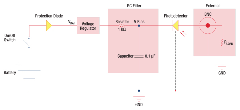
Figure 2: Reverse-Biased Circuit (DET Series Detectors)
The DET series detectors are modeled with the circuit depicted above. The detector is reverse biased to produce a linear response to the applied input light. The amount of photocurrent generated is based upon the incident light and wavelength and can be viewed on an oscilloscope by attaching a load resistance on the output. The function of the RC filter is to filter any high-frequency noise from the input supply that may contribute to a noisy output.
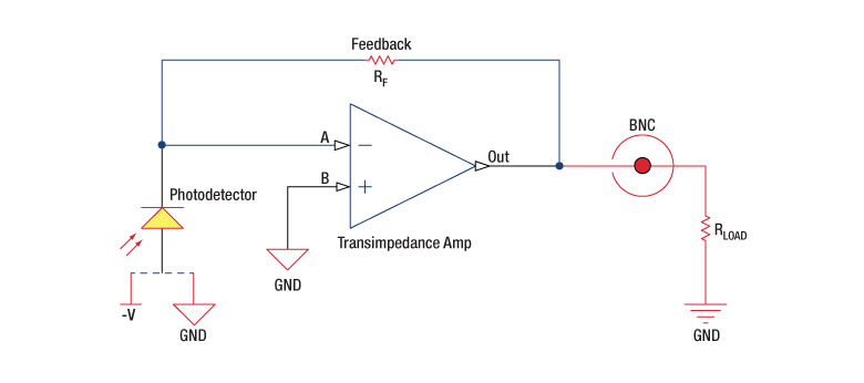
Figure 3: Amplified Detector Circuit
One can also use a photodetector with an amplifier for the purpose of achieving high gain. The user can choose whether to operate in Photovoltaic of Photoconductive modes. There are a few benefits of choosing this active circuit:
- Photovoltaic mode: The circuit is held at zero volts across the photodiode, since point A is held at the same potential as point B by the operational amplifier. This eliminates the possibility of dark current.
- Photoconductive mode: The photodiode is reversed biased, thus improving the bandwidth while lowering the junction capacitance. The gain of the detector is dependent on the feedback element (Rf). The bandwidth of the detector can be calculated using the following:
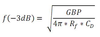
where GBP is the amplifier gain bandwidth product and CD is the sum of the junction capacitance and amplifier capacitance.
Effects of Chopping Frequency
The photoconductor signal will remain constant up to the time constant response limit. Many detectors, including PbS, PbSe, HgCdTe (MCT), and InAsSb, have a typical 1/f noise spectrum (i.e., the noise decreases as chopping frequency increases), which has a profound impact on the time constant at lower frequencies.
The detector will exhibit lower responsivity at lower chopping frequencies. Frequency response and detectivity are maximized for
![]()
Dark Current as a Function of Temperature or Reverse-Bias Voltage
Measurements of dark current as a function of temperature and dark current as a function of reverse-bias voltage were acquired for several packaged detectors. As is described in the following section, dark current is a relatively small electrical current that flows in
One set of measurements were taken for silicon (Si), germanium (Ge), and indium gallium arsenide (InGaAs) reverse-biased photodiodes over temperatures from 10 °C to 50 °C, and another set of measurements were taken for the same detectors while they were held at 24 °C and the reverse-bias voltage varied from 0 to 10 V. Please click the "More [+]" labels in the following expandable tables to read about the experiments and our measurements.
Current-Voltage Characteristics of p-n Junction Photodiodes
The characteristic current-voltage relationship of p-n junction photodiodes includes a forward-biased and a reverse-biased voltage regime. Operation of p-n junction photodiodes occurs in the reverse-biased voltage regime, in which a potential difference is applied across the diode to resist the flow of current. A convenient feature of some packaged photodiodes is that a battery inserted into the package can supply the reverse-bias voltage. Ideally, if no light is incident on a reverse-biased photodiode, no current flows.
Under real-world conditions, random processes in the semiconductor material of the photodiode always generate current carriers (electrons and holes) that produce current. These current generation processes are not driven by the photogeneration of electrons and holes. Instead, they are largely driven by the thermal energy contained in the semiconductor material [1]. This dark current is generally small, but it is present when the photodiode is reverse biased and not illuminated. Dark current magnitudes vary for photodiodes of different material compositions; the efficiencies of the thermal generation processes depend on the type and crystal quality of the semiconductor used in the detector's sensing head. The magnitude of the dark current can be expected to increase as the temperature of the photodiode increases and as the reverse-bias voltage applied to the photodiode increases.
It is important to note that if the reverse bias voltage is increased beyond a certain threshold, the photodiode will suffer reverse breakdown, in which the magnitude of the current increases exponentially and permanent damage to the diode is likely. For this reason, many of the Thorlabs DET packages include a voltage regulator to prevent the bias voltage from reaching breakdown.
When a photodiode is illuminated, the current generated by the incident light adds to the dark current. The carriers in the photocurrent are generated by the energy contained in the photons of the incident light. Above a certain illumination threshold intensity, the magnitude of the photocurrent exceeds the magnitude of the dark current. When the photocurrent is larger than the dark current, the magnitude of the photocurrent can be calculated by measuring the total current and then subtracting the contribution of the dark current. When the photocurrent is smaller than the noise on the dark current, the photocurrent is undetectable. Because of this, it is desirable to minimize the levels of dark current in photodiodes.
[1] J. Liu, Photonic Devices. Cambridge University Press, Cambridge, UK, 2005
| Dark Current as a Function of Temperature |
|---|
|
Dark currents were measured over temperatures of 10 °C to 50 °C for three representative packaged detectors: the Si-based DET100A (previous generation), the Ge-based DET50B (previous generation), and the InGaAs-based DET10C (previous generation). 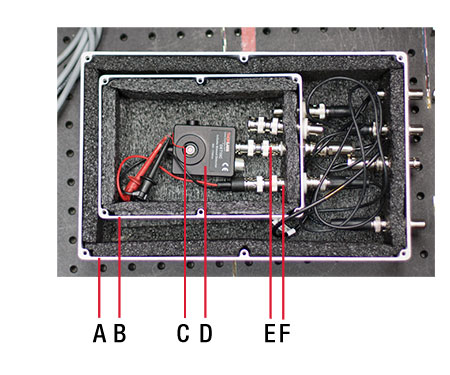 Click to Enlarge Figure 1: The Nested Metal Box Test Fixture with Covers Removed and DET10C Installed Black insulating foam lines the interiors of both boxes. A: Outer Aluminum Box; B: Inner Aluminum Box; C: Thermistor; D: DET10C; E: BNC-to-Triax Feedthrough; F: BNC-to-BNC Feedthrough Experimental Setup As the dark current depends to some degree on the magnitude of the reverse-bias voltage, care was taken to ensure the reverse-bias voltage remained constant over the duration of each measurement set. For these detectors, the source of the reverse-bias voltage was a battery. Before each data set was acquired, the detector's A23 battery was replaced with a fresh one. The battery's voltage was also measured before and after each test to ensure the bias voltage remained constant over the course of the measurement. Thermistors were used to monitor the temperatures of each photodiode continuously during the experiment. A thermistor was held in contact with the outer surface of the TO can housing using a piece of thermal tape. With the thermistor in place, it was not possible to use the detector cap to block light from reaching the photodiode. The detector enclosure consisted of a pair of nested aluminum metal boxes, which are shown with their covers off in Figure 1. Only one box would be required to create a light-tight environment for the photodiode, but an outer box was included in the setup to shield the inner box from EMI related noise. The detector was placed inside the inner box, which was equipped with a BNC-to-triax adapter feedthrough; the BNC end was accessible from the inside of the box, and the triax end was accessible from the outside of the box. The BNC connector on the detector was attached directly to the BNC end of the adapter, which advantageously eliminated the need to use a BNC cable. BNC cables are poorly shielded, and using one could introduce noise from EMI sources to the signal read from the detector. This inner metal box was placed inside of an outer metal box, which possessed a triax-to-triax feedthrough. A triax cable was used to route the detector signal between the feedthroughs on the inner and outer boxes. A triax cable was also used to connect the Keithley 6487 ammeter to the end of the Triax-to-Triax feedthrough accessible on the outside of the outer box. The outer metal box served to isolate the inner metal box from EMI, and the triax cables shielded the detector signal from EMI. After covering two boxes with their respective lids, the nested box set was placed inside an ESPEC ESX-3CW temperature chamber. The ammeter was located outside of the chamber. The electrical connection between the thermistor and TSP01 temperature logger was performed using BNC cables, BNC-to-BNC bulkhead feedthroughs to route the signal out of the nested boxes, and a custom BNC-to-phono jack cable to connect to the temperature logger. Experimental Results The data curves plotted in Figure 2 show the InGaAs-based detector exhibited the least amount of dark current and the Ge-based detector exhibited the most, with the levels of the latter being approximately 5 orders of magnitude higher. In all cases, the dark current increased with the temperature of the photodiode, as expected. The individual points on this graph, plotted as diamonds, are the values of the dark current specified for each detector at 25 °C. These points specify a maximum value of dark current at 25 °C; each diode's dark current must be equal to or less than this value at 25 °C, but the dark current may exceed this specification at higher temperatures, as is the case for the measured DET50B detector. 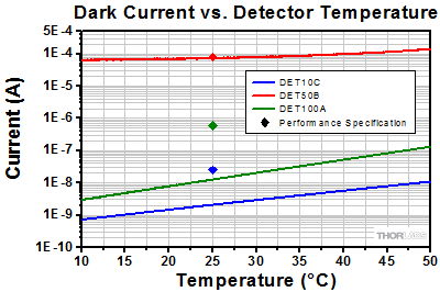 Click to Enlarge Figure 2: Dark Current Data Measured for Three Packaged Photodiodes The discrete data points, plotted as diamonds, are values of the dark current specified for each detector at 25 °C. 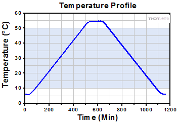 Click to Enlarge Figure 3: Temperature of a Representative Photodiode Controlled by the Conditions in the Environmental Chamber Dark current measurements were acquired between 10 °C and 50 °C (indicated by the shaded region) and are plotted in Figure 2 . Experimental Limitations |
| Dark Current as a Function of Reverse-Bias Voltage |
|---|
|
Dark currents were measured while three representative packaged detectors, the Si-based DET100A (previous generation), the Ge-based DET50B (previous generation), and the InGaAs-based DET10C (previous generation), were held at 24 °C and their reverse-bias voltages were varied between 0 and 10 V. Either a battery or an external power supply, such as the DET2B Power Adapter Bundle, can be used to provide the required reverse-bias voltage. The measurements described below were made to demonstrate the change in dark current as the voltage supplied by the battery decreases from battery drainage. 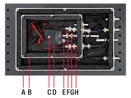 Click to Enlarge Figure 1: The Nested Metal Box Test Fixture with Covers Removed and DET10C Installed Black insulating foam lines the interiors of both boxes. A: Outer Aluminum Box; B: Inner Aluminum Box; C: Thermistor; D: DET10C; E: Power Adapter of the DET1B Power Supply; F: BNC-to-BNC Feedthrough for the DET1B, G: BNC-to-Triax Feedthrough for the Detector Signal; H: BNC-to-BNC Feedthrough for the Thermistor Experimental Setup The detector enclosure consisted of a pair of nested aluminum metal boxes, which are shown with their covers off in Figure 1. Only one box would be required to create a light-tight environment for the photodiode, but an outer box was included in the setup to shield the inner box from EMI related noise. The detector was placed inside the inner box, and electrical connections were made through it using BNC and BNC-to-triax adapter feedthroughs. The measurement signal from the detector was routed through the BNC-to-triax adapter feedthrough. The BNC connector on the detector was attached directly to the BNC end of the adapter, which advantageously eliminated the need to use a BNC cable. BNC cables are poorly shielded, and using one could introduce noise from EMI sources to the signal read from the detector. This inner metal box was placed inside of an outer metal box, which possessed a triax-to-triax feedthrough. A triax cable was used to route the detector signal between the feedthroughs on the inner and outer boxes. A triax cable was also used to connect the Keithley 6487 ammeter to the end of the Triax-to-Triax feedthrough accessible on the outside of the outer box. The outer metal box served to isolate the inner metal box from EMI, and the triax cables shielded the detector signal from EMI. After covering the two boxes with their respective lids, the nested box set was placed inside an ESPEC ESX-3CW temperature chamber. The ammeter was located outside of the chamber. A DET1B (previous generation, current generation DET2B), which includes a power supply and a power adapter designed to be inserted into the battery port of the DET series detectors, was used to supply the reverse-bias voltage, which was routed through BNC feedthroughs. The power adapter was inserted into the detector, and the opposite end of the adapter was connected to a BNC feedthrough fitted into the wall of the inner box. A BNC cable and another feedthrough were used to extend the electrical connection to the outside of the outer box, and the voltage output of the Keithley 6487 was connected to that. A computer was interfaced with the Keithley, which allowed the computer to simultaneously control the reverse-bias voltage while measuring the dark current. As the dark current depends strongly on temperature, thermistors were used to monitor the temperatures of each photodiode continuously during the experiment. A thermistor was held in contact with the outer surface of the TO can housing using a piece of thermal tape. With the thermistor in place, it was not possible to use the detector cap to block light from reaching the photodiode. The electrical connection between the thermistor and TSP01 temperature logger was performed using BNC cables, BNC-to-BNC bulkhead feedthroughs to route the signal out of the nested boxes, and a custom BNC-to-phono jack cable to connect to the temperature logger. Experimental Results The Si-based DET100A does not contain an integrated voltage regulator, while both the Ge-based DET50B and the InGaAs-based DET10C do. Voltage regulators integrated into photodiodes are used to maintain a stable reverse bias voltage across the photodiode. In general, voltage regulators are applied in a range of applications to automatically maintain a stable voltage level: the regulator ensures that the output voltage level is approximately constant as long as the voltage input falls within a specified range. When the input voltage decreases below the voltage regulator's dropout voltage, which marks the lower end of the range, the regulator is no longer able to regulate the output voltage. As the input voltage continues to decrease from the dropout voltage, the output voltage decreases until a threshold is reached and the regulator becomes non-functional. While in this off state, the output voltage is negligible. In the case of the Ge-based DET50B and the InGaAs-based DET10C, the output voltage provided by the voltage regulator is used to reverse bias the photodiode. The absence of a voltage regulator in the Si-based DET100A results in its measured dark current, plotted in Figure 2, continuing to increase as the voltage supplied by the Keithley 6487 increases. The dark current measured for the DET100A increases exponentially up to a reverse-bias voltage of 0.5 V, and then it increases linearly for reverse-bias voltages between approximately 0.5 V and 10 V. A fresh battery supplies ≥10 V. Both the Ge-based DET50B, shown in Figure 3, and the InGaAs-based DET10C, shown in Figure 4, exhibit no dark current until the reverse-bias voltage reaches a threshold (approximately 1 V for the DET50B and 1.5 V for the DET10C). The voltage range up to this threshold value corresponds to the off state of the voltage regulator. After this threshold is exceeded, the dark currents measured for these detectors increase, approximately exponentially, until the voltage supplied by the Keithley 6487 reaches the dropout regulator voltage of 5.5 V. For supplied voltages between 5.5 V and 10 V, the voltage regulator maintains a constant 5.5 V reverse-bias across the photodiodes, which results in an approximately constant values of dark current for supplied voltages over this range. As a fresh battery supplies ≥10 V, the voltage regulator has the effect of ensuring the dark current level remains approximately constant over much of the battery's lifetime, as well as protecting the photodiode from exposure to excessive reverse-bias voltages in general. 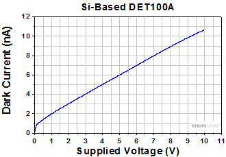 Click to Enlarge Figure 2: Dark current data measured for the Si-based DET100A packaged photodiode, which does not include an integrated voltage regulator, is plotted as a function of the voltage supplied by the Keithley 6487. 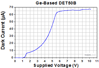 Click to Enlarge Figure 3: Dark current data measured for the Ge-based DET50B packaged photodiode, which includes an integrated voltage regulator, is plotted as a function of the voltage supplied by the Keithley 6487. 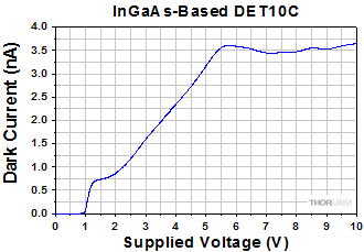 Click to Enlarge Figure 4: Dark current data measured for the InGaAs-Based DET10C packaged photodiode, which includes an integrated voltage regulator, is plotted as a function of the voltage supplied by the Keithley 6487. Experimental Limitations |
About Our Lab Facts
Our application engineers live the experience of our customers by conducting experiments in Alex’s personal lab. Here, they gain a greater understanding of our products’ performance across a range of application spaces. Their results can be found throughout our website on associated product pages in Lab Facts tabs. Experiments are used to compare performance with theory and look at the benefits and drawbacks of using similar products in unique setups, in an attempt to understand the intricacies and practical limitations of our products. In all cases, the theory, procedure, and results are provided to assist with your buying decisions.
The following table lists Thorlab's selection of previous and current generation PDA, PDF, and DET detectors.
| Previous Generation Cross Reference of PDA and DET Detectors | |||||
|---|---|---|---|---|---|
| Wavelength | Material | Biased Detector |
Amplified Detector |
||
| Current Generation | Previous Generation | Current Generation | Previous Generation | ||
| 200 - 1100 nm | Si | DET10A2 | DET10A(/M) | PDA10A2 | PDA10A(-EC) |
| 320 - 1000 nm | Si | - | - | PDA8A2 | PDA8A |
| 400 - 1000 nm | Si | - | - | PDA015A2 | PDA015A(/M) |
| 320 - 1100 nm | Si | DET100A2 | DET100A(/M)a | PDA100A2 | PDA100A(-EC)b |
| Si | - | - | PDF10A2 | PDF10A(/M) | |
| 350 - 1100 nm | Si | DET36A2 | DET36A(/M) | PDA36A2 | PDA36A(-EC) |
| 500 - 1700 nm | InGaAs | DET10N2 | DET10N(/M) | - | - |
| 800 - 1700 nm | InGaAs | DET20C2 | DET20C(/M) | PDA20CS2 | PDA20CS(-EC) |
| - | - | PDA05CF2 | PDA10CF(-EC) | ||
| - | - | PDA015C2 | PDA015C(/M) | ||
| - | - | PDF10C2 | PDF10C(/M) | ||
| - | - | PDA20C2 | PDA20C(/M) | ||
| 800 - 1800 nm | Ge | DET30B2 | DET30B(/M) | PDA30B2 | PDA30B(-EC) |
| DET50B2 | DET50B(/M) | PDA50B2 | PDA50B(-EC) | ||
| 900 - 1700 nm | InGaAs | DET10C2 | DET10C(/M) | PDA10CS2 | PDA10CS(-EC) |
| 900 - 2600 nm | InGaAs | DET05D2 | DET05D(/M)c | PDA10D2 | PDA10D(-EC)c |
| DET10D2 | DET10D(/M)c | - | - | ||
Pulsed Laser Emission: Power and Energy Calculations
Determining whether emission from a pulsed laser is compatible with a device or application can require referencing parameters that are not supplied by the laser's manufacturer. When this is the case, the necessary parameters can typically be calculated from the available information. Calculating peak pulse power, average power, pulse energy, and related parameters can be necessary to achieve desired outcomes including:
- Protecting biological samples from harm.
- Measuring the pulsed laser emission without damaging photodetectors and other sensors.
- Exciting fluorescence and non-linear effects in materials.
Pulsed laser radiation parameters are illustrated in Figure 1 and described in the table. For quick reference, a list of equations is provided below. The document available for download provides this information, as well as an introduction to pulsed laser emission, an overview of relationships among the different parameters, and guidance for applying the calculations.
|
Equations: |
||||
 |
and |  |
||
 |
||||
 |
||||
 |
||||
Peak power and average power calculated from each other: |
||||
 |
and |  |
||
| Peak power calculated from average power and duty cycle*: | ||||
 |
*Duty cycle ( ) is the fraction of time during which there is laser pulse emission. ) is the fraction of time during which there is laser pulse emission. |
|||
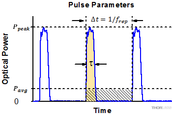
Click to Enlarge
Figure 1: Parameters used to describe pulsed laser emission are indicated in the plot (above) and described in the table (below). Pulse energy (E) is the shaded area under the pulse curve. Pulse energy is, equivalently, the area of the diagonally hashed region.
| Parameter | Symbol | Units | Description | ||
|---|---|---|---|---|---|
| Pulse Energy | E | Joules [J] | A measure of one pulse's total emission, which is the only light emitted by the laser over the entire period. The pulse energy equals the shaded area, which is equivalent to the area covered by diagonal hash marks. | ||
| Period | Δt | Seconds [s] | The amount of time between the start of one pulse and the start of the next. | ||
| Average Power | Pavg | Watts [W] | The height on the optical power axis, if the energy emitted by the pulse were uniformly spread over the entire period. | ||
| Instantaneous Power | P | Watts [W] | The optical power at a single, specific point in time. | ||
| Peak Power | Ppeak | Watts [W] | The maximum instantaneous optical power output by the laser. | ||
| Pulse Width |  |
Seconds [s] | A measure of the time between the beginning and end of the pulse, typically based on the full width half maximum (FWHM) of the pulse shape. Also called pulse duration. | ||
| Repetition Rate | frep | Hertz [Hz] | The frequency with which pulses are emitted. Equal to the reciprocal of the period. | ||
Example Calculation:
Is it safe to use a detector with a specified maximum peak optical input power of 75 mW to measure the following pulsed laser emission?
- Average Power: 1 mW
- Repetition Rate: 85 MHz
- Pulse Width: 10 fs
The energy per pulse:

seems low, but the peak pulse power is:

It is not safe to use the detector to measure this pulsed laser emission, since the peak power of the pulses is >5 orders of magnitude higher than the detector's maximum peak optical input power.
| Posted Comments: | |
Heonsik Lee
(posted 2024-07-03 17:20:30.483) Hi,
I'm Heonsik Lee, from KAIST, Korea.
Is the output of 'DET100A2' a current or voltage?
I use the oscilloscope for measuring the voltage with T-connector with 50 ohm terminator, but no signal measured; rather, if I connect the PD-oscilloscope directly with a BNC cable, I can measure the voltage.
And, also I want to know the maximum output. the manual said maximum current is 10 mA, and maximum output is 9V(HI-Z), 170 mV(50 ohm). is it linearly related to min-max laser power? ksosnowski
(posted 2024-07-03 10:59:01.0) Hello Heonsik, thanks for reaching out to us. The DET series output photocurrent in response to applied light. The impedance of the measurement acts as a gain factor to voltage conversion so with 50 Ohm termination you see a fairly low 50 V/A. A higher impedance can be used for higher gain at a direct cost to the bandwidth of the detector. Your observation is very common for customers using a scope with a high input impedance. The maximum output current should be kept below 10mA to avoid damaging the microwires on the photodiode in any scenario. With high impedance though, you will experience saturation before reaching 10mA of photocurrent. Saturation will occur slightly above the bias level of the detector used and can cause the photodiode to degrade as photons can only convert to heat at this point, making the power measurement nonlinear as well. The 170mV you reference is in regards to the battery check function of the detector and is due to the current limiting resistor applied by the battery check button. Using an impedance much larger 2540 Ohm will allow you to read the entire battery voltage directly, and if only 9V can be measured though the battery check, we would consider the battery exhausted. Birgit Lange
(posted 2024-06-20 07:10:31.57) Sorry, but I could not find the maximum peak optical input power for the DET10D2.
Could you please give me this value (wavelength: 1940nm).
Thank you very much for your help!
Kind regards,
Birgit Lange ksosnowski
(posted 2024-06-25 06:04:08.0) Hello Birgit, thanks for reaching out to Thorlabs. The maximum power of the DET series is limited by either saturation or photocurrent limits depending on the situation. There is also more detail on this in the previous feedbacks. DET10D2's maximum photocurrent rating is 5mA, and by estimating the typical responsivity around 1940nm as 1.3A/W, this gives a practical upper limit of 3.85mW with 50 Ohm termination, or less with higher impedance values where one would experience saturation. If you consider a 1MOhm impedance measurement, then at 1000000 V/A, you would surpass the 1.8V bias of DET10D2 closer to 1.4uW. I have reached out directly to discuss this in further detail. Xianghe Wang
(posted 2024-05-02 22:28:15.937) 我想知道怎么查看每款型号的最大可探测功率 ksosnowski
(posted 2024-05-02 12:44:44.0) Hello Xianghe, thanks for reaching out to Thorlabs. The maximum power of the DET series is limited by either saturation or photocurrent limits depending on the situation. Saturation occurs relative to the detector's fixed bias voltage, so the optic power that leads to saturation also depends on the diode's spectral responsivity, and the measurement load used. High impedance measurements provide higher gain but it is easy to saturate at lower powers with the 1MOhm impedance common to oscilloscopes. 50 Ohm termination, as required for the full detector bandwidth, leads to a gain of 50 V/A, and in this case one typically will hit the max current output of the DET well before reaching saturation across the smaller load. Exceeding the photocurrent limits can burn out the microwires connecting the diode. We do not have a surface damage threshold for the photodiodes however this would be well past saturation if using at least 80% of the active area of these devices. As both these limits depend on the wavelength and measurement load of the application, we do not specify a single maximum optical power level directly. Your local tech support team has reached out to discuss this further. Echo Liang
(posted 2024-03-20 15:41:24.057) 您好,之前在thorlabs购买了DET100A/M产品想知道它的上升时间是多少。目前在网站上没有相关信息被DET100A2替代。 ksosnowski
(posted 2024-03-20 12:01:35.0) Hello Echo, thanks for reaching out to Thorlabs. DET100A used a slightly different diode than our current DET100A2 model. The device manual and specs can still be found by searching our site for DET100A. With a 50 Ohm load and fresh 12V A23 battery, the rise time is specified as 43ns. Above 800nm in large-area silicon detectors (10mm x 10mm, 3.6mm x 3.6mm) we have noted an increased rise time as you go deeper into the NIR range. A member from your local tech support team has reached out directly to discuss this further. Alexander Voronov
(posted 2024-01-11 16:21:49.237) Hi.
In our application the space is constrained, DET100A2 doesn't fit to it. Could you make a product similar to SM1PD1B(mount), but with the photodiode characteristics like DET100A2 (with externally provided bias)?
Thank you! ksosnowski
(posted 2024-01-11 10:26:50.0) Hello Alexander, thanks for reaching out to Thorlabs. We offer PBM42 bias module which can be connected via coax cable between the SM1PD1B and your measurement to apply an external bias, making a similar system to the DET series. We do also offer PDAPC2 which is an OEM style photodiode, bias, and amplifier circuit on a compact PCB for integration in systems like this. However, there isn't much space for pushing the bias RC filter and connection into the mounted photodiode housing itself. I have reached out directly to discuss this application further. Mirko Campo
(posted 2024-01-10 15:23:05.887) Dear Sir,
I have a DET10A2 detector. What is its maximum peak optical input power? Thank you for your attention. ksosnowski
(posted 2024-01-10 01:17:48.0) Hello Mirko, thanks for reaching out to us. DET10A2 has a 10mA max photocurrent limit so near the peak of responsivity 0.44 A/W this would be roughly 20mW. If using a larger load like 1MOhm, you may hit the 10V bias and saturation point at even lower photocurrent levels due to Ohm's law. A low battery will lower the bias and saturation point as well. If you are saturating the sensor, then use a lower load resistance or less optic power to keep the response linear. Saturation causes the sensor to degrade ultimately resulting in an increased dark device current. mark d
(posted 2023-06-13 11:29:39.743) This detector, DET36A2, and others we have from Thorlabs, has a "battery check" button, but I have found no instructions how to use it. I push it, but nothing seems to change. How is it supposed to work? ksosnowski
(posted 2023-06-13 01:00:49.0) Hello Mark, thanks for reaching out to Thorlabs. Page 7 of the DET36A2 manual covers the setup for battery measurements to check the bias. We recommend measuring the battery with a high impedance device. Many oscilloscopes have a HiZ setting and/or channel for this. As covered in the manual, using small loads will effect the measurement due to the current limiting resistor in the DET36A2. A low battery will result in reduced bandwidth and a lower saturation point. I have reached out directly to discuss this further. Robert McCoy
(posted 2023-06-12 12:33:01.31) Greetings,
Can you tell me what photodiode is used in the Det100A2 biased SI detector?
Thanks and regards,
Bob ksosnowski
(posted 2023-06-13 01:03:12.0) Hello Robert, thanks for reaching out to Thorlabs. Unfortunately the exact photodiode used in DET100A2/PDA100A2 is considered proprietary. However our closest bare photodiode is the silicon-based FDS1010. I have reached out directly to discuss your application in more detail. Yutong Feng
(posted 2023-03-30 10:47:48.087) Hello,
I have a DET10C2 and its output current is 0-5mA. I use a 50 ohm BNC cable to connect the detector and oscilloscope. The oscilloscope is set to DC50 ohm coupling. In this configuration, is 250 mV the maximum voltage reading on the scope before the DET10C2
is saturated?
Thank you. ksosnowski
(posted 2023-04-03 01:43:37.0) Hello Yutong, thanks for reaching out to Thorlabs. This max current rating is due not to saturation but limits on the wire bonds of the photodiode. Exceeding this level of photocurrent can result in device failure directly. Ohm's law will determine the voltage this occurs at based on your load resistance. Saturation will occur at a voltage equal to the bias; 5V for DET10C2. In practice, with 50 Ohm you will hit the photocurrent limit before reaching saturation voltage. With higher loads, saturation will occur with less photocurrent due to Ohm's law. We generally do not specify an optical saturation point directly since it varies with load and wavelength. Please note the DET series battery check feature can produce up to 10V in HiZ as noted in the DET manual. Alberto Hohenzollern
(posted 2023-03-21 08:39:16.047) Hello, we would like to use the photodetector DET20X2 for 850 nm photodetection requiring high saturation power (> 3 mW), low noise and low bandwidth (3 - 5 MHz would be sufficient). We were thinking of using a relatively high load resistor at the output ( 500 Ohm - 5 kOhm) to reduce the Johnson NEP, but we are not sure about the bandwidth that we could achieve in our scenario. From the manual, it seems like the dominant term for limiting the bandwidth is the sheet resistance, but it is not clear what the diffusion time constant would be at 850 nm. Could you provide some rough numbers clarifying the bandwidth of the photodetector at 850 nm? Thanks! ksosnowski
(posted 2023-04-25 11:54:28.0) Hello Alberto, thanks for reaching out to Thorlabs. The sheet resistance and diffusion time constant are dominating terms for bandwidth over the NIR range of this detector. The DET20X2 manual's bandwidth section covers this effect and equations to model in greater detail. These effects start around 800nm, and while we have not yet fully swept the upper wavelengths to poll bandwidth, we do have some limited data in this range to share. I have reached out directly to discuss this in further detail. Daniel Aponte
(posted 2023-01-18 11:40:41.107) Hi, I am using a DET10A2 to test a Shutter (AOM) with a UV laser 365nm WL. What we see is a very hi oscillating signal on the Oscilloscope. I wonder if you have a way to test.
If have a graph reference to WL and V-out or any other data can be used to. ksosnowski
(posted 2023-01-25 01:59:18.0) Thanks for reaching out to Thorlabs. The DET10A2 manual, page 13, has the Spectral Responsivity in A/W across the wavelength range of this detector. This can be used to relate the photocurrent to the input light level. Ambient lights can couple to the sensor if it is not shielded, and often result in a 60Hz signal which matches the mains frequency. Page 7 has the equation for bandwidth and rise time, which will depend on the load resistance and diode capacitance (i.e. bias); as well as the output voltage equation, which also depends on load resistance, and generated photocurrent from the sensor. Roger Putnam
(posted 2022-09-22 13:38:06.563) Greetings,
Can you send a graph of the pulse response of DET36A2 (actually want it for obsolete DET36A). Specifically we're interested in the turn-off behavior, both the speed of turn-off, and especially the slow (low) tail that is unfortunately common in fast detectors.
Question 2: Is the slow, low tail in the detector turn-off badly affected if too much light intensity is used on the detector?
Thanks,
Roger ksosnowski
(posted 2022-09-29 02:49:42.0) Thanks for reaching out to Thorlabs. We do not have an exact impulse response plot for the DET36A/A2 models, however we verify the rise time directly on these units in production. These use the FDS100 photodiode which we expect to have a similar rise and fall time. Other diodes like FDS015 have a much longer fall time than their rise. Saturating the detectors can negatively effect the bandwidth and rise/fall time of the detectors by increasing the effective resistance. I have reached out directly to discuss this further. Jaden Lee
(posted 2022-07-28 14:42:48.247) In specifications(DET10A2), the rise time means data acquisition rate?
for example, the DET10A2' rise time is 1 ns
1ns = 1e-9 sec => 10e9 hz = 1000000 khz = 1000 mhz
the DET10A2' data acquisition rate is 1000 mhz ? ksosnowski
(posted 2022-07-28 04:43:26.0) Thanks for reaching out to Thorlabs. Our detectors output an analog signal continuously. The measured rise time describes how long it takes for the active area to respond to an input optical signal and charge up from ~0V. This is due to capacitance and resistance in the photodiode and measurement system. Biased Photodiodes lower this capacitance for a faster response. A lack of bias voltage, or extra system capacitance i.e. due to cabling can negatively effect the response time and bandwidth. The bandwidth for each unit is calculated for an analog sine wave, for other waveforms it will be lower. Square waves for example will take roughly 10x the bandwidth of a sine wave at same frequency to preserve definition. Anton Ryzhov
(posted 2022-05-17 15:51:45.58) Dear Thorlabs team,
why has DET25K2 been discontinued? I do not see an adequate substitution in your actual DET-range... ksosnowski
(posted 2022-05-23 12:31:47.0) Unfortunately we had to discontinue all of our GaP based sensors as this type of diode is no longer being produced. Currently we do not have a direct alternative for this UV performance however we are hoping to replace this with a UV-enhanced Silicon based sensor in the future. We aim to cover a similar UV wavelength range while maintaining device performance. We do not yet have a timeline for this new product. Mark Johnston
(posted 2021-07-12 15:35:34.73) What is the window material on the DET10A2 detector? Can you get one without a window? Thanks. YLohia
(posted 2021-07-13 08:53:32.0) Hello, the window is made of Quartz, nominally 0.5 mm thick. Custom items can be requested by emailing techsales@thorlabs.com. We will discuss the possibility of offering a version of this without the window directly. Mark Johnston
(posted 2021-07-12 15:32:54.307) What is the response time of the DET10A2 detector, i.e. the time from light in to electrical signal out? Thanks. YLohia
(posted 2021-07-13 08:53:30.0) We cannot directly measure the signal propagation time (e.g. the time it takes for the signal to get from the active area to the BNC output), but we have measured the total propagation time of the DET10A2 and a laser diode system. The optical path distance, electrical cable lengths, and oscilloscope delay have been subtracted off, so this value (3 ns for the DET10A2) is the sum of the DET propagation time and the Bias-T/laser propagation time. Most of the delay time is from the DET. The test was performed using a LP915-SF40 diode modulated via the bias-T in an LDM9LP mount using a square wave pulse with a ~5 ns rise time. The diode was always kept above the lasing threshold. Pulse amplitude and DC offset did not seem to have an impact, but some of our customers have noted that this value may shift with the ambient conditions though we don't have a measure of this shift. Morris Wang
(posted 2021-03-28 00:21:58.183) Dear Sir,
I’m writing to enquire about the product DET36A application. I need the DET to detect the pulse laser signal. The signal is served as external trigger (connect to DAQ from TI), in my experiment. However, i cant acquire any signal from DET if i connect it through BNC cable to the external trigger port (Impedence :1M ohm) . Is there anything i could try?
Best wishes,
Morris asundararaj
(posted 2021-04-01 10:27:28.0) Thank you for contacting Thorlabs. We recommend terminating into a 50 Ω load for fast performance. I have reached out to you directly to troubleshoot for your application. sende wang
(posted 2020-11-30 22:11:13.667) I have a DET100A/M detector. Does it have max peak power? Can I use a 5mW laser pointer direct irradiate this detector? asundararaj
(posted 2020-12-16 10:52:20.0) Thank you for contacting Thorlabs. Unfortunately, we do not have an official spec on the damage threshold of the DET100A(2). That being said, the damage to the active area would happen several orders of magnitude above saturation. The saturation power at a certain wavelength can be estimated from the following equation where the max voltage is 10 V (Bias Voltage) and the responsivity is dependent on the wavelength of operation and the terminating resistance is whatever termination is used before the oscilloscope. For fast performance, we recommend a 50 Ω termination. Saturation Power = Max Voltage / (Responsivity *Terminating Resistance). Additionally, one must double check the total current going through the photodiode, as it's possible that the power will be limited by the current rating for the photodiode, which in this case is 10 mA - Maximum Current (in A) = Maximum Optical Power (in W) * Responsivity (in A/W) Josh Josh
(posted 2020-01-10 06:48:33.143) Dear Thorlabs,
What is the measurement uncertainty of the detectors, more specifically the DET10C2 detector?
Best regards,
Josh YLohia
(posted 2020-01-10 11:02:07.0) Hello Josh, thank you for contacting Thorlabs. The DET series of detectors do not have a particular "uncertainty" associated with them because these are not calibrated devices. They output a certain voltage to be measured on the oscilloscope and this is not a calibrated value. ding zhang
(posted 2019-11-20 14:20:01.777) DET50B2
1.The detector can measure the current no matter what the state of the switch , whether it is normal or not
2,Turn off the switch during the test
What is the correct operation flow when the current drops and then rises asundararaj
(posted 2019-11-21 09:03:52.0) Thank you for contacting Thorlabs. When the switch on the detector is turned off, the detector will be operated in photovoltaic mode, and will still be able to detect light. Please note that the specifications are estimated when operated in the photoconductive mode, i.e. with the switch turned on. jongmin lim
(posted 2019-08-21 13:14:55.94) hello,
i'm currently using det36 to measure laser intensity changes. in the same time, i also have to scan the beam which is images on the sensor of photodiode. though i imaged the scanned light, it slightly be moved in the active area of the sensor. is it may induce an additional noise (or differences)? in short, is there a position dependent sensitivity in the active area? YLohia
(posted 2019-08-21 09:54:48.0) Hello, thank you for contacting Thorlabs. Yes, the response of a photodiode is dependent on the position of the incident beam. Please see detailed information regarding this in our Lab Fact here : https://www.thorlabs.com/newgrouppage9.cfm?objectgroup_id=10741&tabname=Spatial%20Uniformity. The DET36A2 contains the same photodiode as the SM05PD1A mentioned in this study. That being said, we have not yet specifically measured the spatial uniformity of a photodiode in terms of NEP. Simon Wall
(posted 2019-07-02 06:33:28.657) Can you comment on the linearity of these detectors?
We have a DET10D2 which we are using to probe the intensity of a femtosecond light beam (5 kHz) that is modulated in a sample (approx 250 Hz).
We believe that we are in the linear regime, but we are finding that the relative modulation amplitude I_max/I_min depends on the IR intensity in the diode. We do not think the sample is behaving non-linearly, so we are wondering if the detector may be. asundararaj
(posted 2019-08-28 04:28:44.0) Thank you for contacting Thorlabs. Since these were not designed for fs applications, we do not have any data for the DET10D2 in this regime. Although, we have had customers successfully use the DET10A2 with a fs beam at 800 nm. Please note that fs pulses will not be individually resolved since the rise time of DET10D2 is typically 25 ns. kyle.j.wilkin
(posted 2019-02-27 11:39:52.427) Hello, I currently have a DET10A and I am using it to try to characterize pre and post pulses from an amplified laser. Currently when I hook it up to a oscilloscope I get what just looks like an over saturated response when shining only disperse reflected light on it. It also seems the resolution is not enough to view the pre or post pulse separate from the main pulse when I believe in the past this was possible. Does the resolution of the photo diode decrease over time? llamb
(posted 2019-03-07 02:08:48.0) Thank you for your feedback. After discussing via email, we determined that the over saturated response you were seeing was caused by the oscilloscope impedance setting being too high, as opposed to a low 50 Ohm impedance. go89yo
(posted 2019-01-28 14:27:03.92) Hello, I am mun seok choe from Ulsan National Institute of Science and Technology (UNIST) in Republic of korea.
I purchased DET10A and DET100A. I connected it to oscilloscope. However, it doesn't work in 50 Ohm resistance in oscilloscope (no response). Only 1Mohm resistance is working.
(I used bnc cable(50ohm,2m) without bnc terminator)
Could you explain that what is problem? Thank you. llamb
(posted 2019-02-06 11:52:41.0) Thank you for your feedback. After troubleshooting by email, we determined that your input optical signal is likely too low to be read above the noise level of these detectors with a 50 Ohm resistance. The high impedance provides a higher measured voltage for a given generated photocurrent. yongqi.shi
(posted 2018-11-25 23:32:06.04) Dear Sir, I'm using a DET10A to measure the rise time of it after a AOM. When I connected an output to 50ohm terminator, it was around 90-100ns (nearly 100 times larger than the nominal value) which is reasonable due to the rise time of AOM. However, when I connected to different terminators of a VT1, it will show different rise time compared with the formula I get from manual. General speaking, they all around 30 times longer than the calculated value (even much longer than AOM rise time). What would be the reason? The BNC cable is around 2 m long. I supposed it influenced the rise time. Do you have a kind of empirical formula to calculate the rise time including the cable length? BTW, I was using the 10%-90% time interval to calculate the rise time, is it compatible with the method you used in the manual? I will greatly appreciate you with your feedback. YLohia
(posted 2019-01-28 10:30:05.0) Hello, thank you for contacting Thorlabs. What's the rise time of your modulator? Have you been able to successfully follow the modulation signal using some other detector in your setup? Would it be possible for you to provide < 30ns modulation directly to your laser and measure that, without using the AOM? Are you using a 50 Ohm coaxial cable? What oscilloscope are you using? I reached out to you via email to troubleshoot this directly. guitar2852
(posted 2018-06-18 21:27:37.37) Dear Sir.
I'm using DET36A at Laser welding monitoring system.
However, it took a damage from reflected laser beam so its performance getting bad.
Therefore, I have a question, what is DET36A2's damage threshold value? and how to prevent it?
BR YLohia
(posted 2018-06-19 11:17:59.0) Hello, thank you for contacting Thorlabs. A conservative value would be ~100 W/cm^2 average power density (but it can be closer to 100 kW/cm^2) or about 100 mW total average power. We don't typically spec a damage threshold for photodiodes for two main reasons: the output voltage will saturate several orders of magnitude before damaging the surface, and usually only CW damage is a concern for most situations.
For pulsed sources, the active area is less prone to pulsed damage mechanisms (e.g. dielectric breakdown/avalanche ionization). The primary damage mechanism is thermal burning at the PN junction. Both CW and pulsed damage will strongly depend on usage conditions.
High speed detectors (e.g. DET08CFC, DET01CFC) do have a max power ratings. This is limited by the max photocurrent which the unit's internal electronics are able to handle. This is not always the same as the CW saturation. user
(posted 2018-04-12 14:01:22.587) Hello,
at what photocurrents do the detectors go into saturation? I was searching for graphs but didn't find any.
I am specially looking at the DET10A2 and the Det36A2.
Kind regards
Michael YLohia
(posted 2018-04-19 04:17:36.0) Hello Michael, thank you for contacting Thorlabs. The saturation threshold of a detector depends on many factors such as diode temperature, load resistance value, beam profile and size, modulation characteristics, wavelength, bias voltage, etc. For more details regarding this, please see our "Lab Fact" on photodiode saturation limits here: https://www.thorlabs.com/images/TabImages/Photodetector_Lab.pdf. We spec a max output current of 10mA for these detectors. There is a resistor in series as a part of an RC filter, thus the 10mA can only be achieved with a pulsed/modulated input (typically <35us pulse width); the saturation current for a CW signal will be lower. Assuming a 50 Ohm load resistance with input at peak responsivity, the theoretical estimates for CW saturation power are ~11mW and ~8mW for DET10A2 and DET36A2, respectively. wenzel.jakob
(posted 2018-04-09 14:51:01.517) I'm curious about the difference between DET100A2 and the DET100A/M that it replaces. YLohia
(posted 2018-04-17 02:28:37.0) Response from Yashasvi at Thorlabs USA: Hello, thank you for contacting Thorlabs. The DET100A2 features both 8-32 and M4 (imperial and metric) tapped mounting holes, while the DET100A/M featured only M4 (metric) tapped hole. Other differences include a redesigned housing and the following performance specifications: the wavelength range changed from 350-1100 nm to 320-1100 nm, peak wavelength from 970 nm to 960 nm, NEP from 2.07 x 10⁻¹³ W/√Hz to 2.4 x 10⁻¹⁴ W/√Hz, dark current from 100 nA to 0.9 nA, and an output voltage of 0-10 V is now an output current of 0-10 mA. The circuit design of the two is the same, however the board itself was changed to accommodate the new housing. The change in these specs is largely due to more rigorous testing on our end, as opposed to the calculated values that we had before. I will reach out to you directly with more information about these differences. yisun7
(posted 2018-02-27 16:18:49.337) The ouput voltage DET10C detector is not linear to the measured power of the same laser beam. Is it normal? tfrisch
(posted 2018-02-28 11:46:41.0) Hello, thank you for contacting Thorlabs. The output current should be linear with respect to the input power under normal operating conditions. If it is not linear, there are a few things to check. First, is the detector terminated to a 50 ohm load? Terminating to a high impedance load will greatly reduce the linear response range and the detector will saturate at lower powers. Second, is the bias working properly? It could be that the battery is dead or it is not making good contact with the spring in the cap. The switch should also be set to 1 rather than 0. Lastly, the photodiode could be saturating. Assuming the bias and load are standard, the output current will be roughly linear with the input power from 0mA output up to a several mA output. The corresponding inputs can be calculated based on the responsivity at your operating wavelength. I will reach out to you directly to discuss this. shivaprasad
(posted 2018-01-02 00:45:52.4) For DET10A, do you have data on how the 3db cutoff frequency decreases with load resistance? (for instance, the bandwidth is 380 MHz for 50 ohm load, what would it be for 500 ohm etc.; an initial guess is it scales linearly?)
Thank you
Shiva tfrisch
(posted 2018-01-02 04:42:22.0) Hello. Thank you for contacting Thorlabs. Yes, a photodiode with a load resistor can be modeled as an RC circuit, so the time constant will increase proportionally to the load resistance. sxogus123
(posted 2017-08-07 16:25:17.857) I am a student studying in Korea.
There is no voltage in the resistor when a resistor is connected in series to the output of DET100A / M. I do not know why this is.
I would like to ask if there is any way to use the circuit using the output of the DET100A / M.
What I want to do is to connect the output of the DET100A / M to the circuit to get an output of 0 to 5V.
I did not think it would be possible to use the voltage distribution law.
Voltage distribution law was used to reduce 0 ~ 10V output proportionally from 0 ~ 5V.
However, when I connected the output of the DET100A / M to the resistor, I found that the voltage was not transmitted.
In my opinion, when connecting two of the same resistors at 10V output, I think 5V should be applied to one resistor, but the desired value does not actually come out.
I would like to ask if there is any way to use the voltage of the DET100A / M output. user
(posted 2017-05-15 10:39:10.12) What is the threshold of destruction of the photodiode? (DET10A) tfrisch
(posted 2017-05-18 08:23:58.0) Hello, thank you for contacting Thorlabs. The damage threshold is not specified because the detector will have a non-linear or saturated response before it is damaged. Please contact TechSupport@Thorlabs.com to discuss further. lars.heinen
(posted 2017-02-23 04:11:42.91) Our DET10N/M PD only has an output voltage of a few mV in saturation with a 50 Ohm RLoad, which is correct according to the responstivity diagram. But the data sheet says it should have an output voltage level of 0-5V with a 50 Ohm RLoad. How is this discrepancy possible?
Also using an amplifier with a factor of 20 the rise time of the photodiode is about 10µs with a 50 Ohm RLoad. tfrisch
(posted 2017-03-03 08:02:27.0) Hello, thank you for contacting Thorlabs. The 0-5V note comes from on older CE standard and corresponds not to the photodiode signal, but the bias battery test mode. Newer versions of the housing are expected to clarify this engraving. As for the rise time, I will reach out to you directly about the specs of your amplifier and your measurement method. ati5770gd5
(posted 2016-12-28 17:13:27.683) This wide range PD works pretty nice in my optical system, especially for us~ns measurement within NIR region, both the sensitivity and response time are so good!
However, i would like to know if i can modulate the Bias voltage (ex: Sine wave input Bias or DC+Sine wave) to achieve the modulation of gain so that i could perform some frequency domain lifetime measurements. tfrisch
(posted 2016-12-30 02:16:37.0) Hello, thank you for contacting Thorlabs. The DET50B/M has a built in bias battery which cannot be varied, but the photodiode is available as a bare diode under the part number FDG50. You can build that into your own setup with a variable bias if needed. I will reach out to you directly as well. kurzn
(posted 2016-12-08 16:04:53.733) Hello,
What is the damage threshold for the PD DET10N/M?
Regards, tfrisch
(posted 2016-12-14 01:49:34.0) Hello, thank you for contacting Thorlabs. While we don't have any damage testing on DET10N/M, the detector we have a non linear, and then saturated response before it is damaged. I will reach out to you directly to discuss this further. cesnike10
(posted 2016-07-22 04:13:16.827) greetings, I am using a photodetector det36a, I record the variations of a tungsteno lamp in a arduino card could suggest a suitable configuration of connections on a port analogous to avoid saturation? user
(posted 2016-06-05 19:24:42.95) Can you tell me how is the resolution of DET36A? I have a 1mW HeNe laser source and want to observe power variation under 0.01mW. besembeson
(posted 2016-06-08 12:35:46.0) Response from Bweh at Thorlabs USA: 0.01mW is well within the resolution capability of the detector. You can estimate this from the detector NEP and your measurement bandwidth. chanjael
(posted 2016-02-16 10:30:43.48) Dear
I have used your photo detector DET10A/M to analyze time resolved electroluminance of OLED(organic light emitting diode).
DET10A/M is connected to oscilloscope with BNC cable and detected the light from OLED applied voltage pulse, 8msec, duty 50%.
Generally, rising and falling time of OLED is known to ~10 usec order. But in my system, rising and falling time is detected in the range of 80~300 usec.
I want to know this reason.
if you send e-mail address,I will send e-mail about my system and results.
Please replay to this reason and I will happy to recommend system.
Thank you besembeson
(posted 2016-03-03 01:14:46.0) Response from Bweh at Thorlabs USA: I will contact you to further discuss this. acook
(posted 2015-12-17 10:17:50.847) Do you have data showing the response of the DET10C and DET10N detectors to a fast step (not pulse) rise or decay? This is needed to evaluate these detectors for secondary response (can be from defects or device architecture), that is how much of the response occurs in the quoted rise time, and how much occurs with a slower response time?
If we purchase one or both of these detectors to do our own test, can we return them if we don't like the secondary response? besembeson
(posted 2015-12-21 05:05:40.0) Response from Bweh at Thorlabs USA: We typically use fast rise times in our tests to validate the bandwidth of the detector but that data is not something we keep for each detector once it meets our specifications. I will contact you regarding details of your application and such tests. adrimshaw
(posted 2015-11-11 10:30:35.257) Is the Det 36A a p-n or p-i-n photodiode? jlow
(posted 2015-11-12 05:00:46.0) Response from Jeremy at Thorlabs: It's PIN type. rbjaculbia
(posted 2015-05-20 03:46:44.56) I believe this is a very elementary question but I just want to clarify something. We want to connect the DET10A to an SR510 lock-in amplifier. Do we still need to add a terminating resistor? Thanks! jlow
(posted 2015-05-21 09:09:23.0) Response from Jeremy at Thorlabs: Reading through the manual for the SR510, you can use the input on the SR510 labeled "I" for current signal without a terminating resistance. aklossek
(posted 2014-12-04 09:14:20.603) Dear ladies and gentlemen,
I have your DET10A detector. In the delivered manual it is written that the NEP is 1.9E-14. That is also written in the catalog. But on your website it is written 1.9E-13.
Please Tell me what is correct?
Best regards
André Klossek myanakas
(posted 2014-12-05 02:36:01.0) Response from Mike at Thorlabs: Thank you for your feedback. The correct value is 1.2 x10^-13. This value is given on the website and in the linked manual. The NEP specification for the DET10A detector was updated in July 2013, so the manual you currently have may be outdated. To download the updated manual click on the red docs icon next to the item number on the webpage. tianzhushang
(posted 2014-10-13 10:55:38.26) Can you tell me the gain of the DET10A/M? jlow
(posted 2014-10-13 08:59:57.0) Response from Jeremy at Thorlabs: The DET series detector do not have an amplifier in the package. The amplified version of the DET10A/M is the PDA10A-EC (http://www.thorlabs.com/newgrouppage9.cfm?objectgroup_id=3257). jmiles02
(posted 2014-10-07 18:11:05.6) I'm using a 100fs, 267nm 1kHz laser and need to monitor the output. I've directed the beam at the DET10A and I am getting an average signal of a few 10's of mV's per second. Looking further I've acquired the signal per laser pulse but it seems to oscillate quite significantly. This leads me to believe it could be something to do with the response time? Is this device suitable for such an application? jlow
(posted 2014-10-08 04:06:30.0) Response from Jeremy at Thorlabs: The detector has a rise time of around 1ns with 50Ohm load so it is definitely not fast enough to characterize your pulse fully. Typically the peak power of a femtosecond laser is also quite high so there could be non-linear response from the DET10A. I will contact you directly to discuss about your application and suggest something suitable. jp
(posted 2014-09-14 15:32:05.983) Hi, this is Junsong Peng from Royal Institute of Technology, Sweden.Could you give me some details about "DET 300"? such as the rise time and wavelength window. I can not find the datasheet elsewhere. Thank you very much. PS:I found that it can detect wavelength around 1900 nm. jlow
(posted 2014-09-18 10:43:40.0) Response from Jeremy at Thorlabs: The DET300 is an old product we used to sell. I will find the datasheet and send it to you. harishkn23
(posted 2014-08-06 03:20:55.467) I need one clarification, what is the p-i-n material used in this photodetector and thickness of those materials?. what is the thickness of SiO2 layer in DET10A photodetector? jlow
(posted 2014-08-06 08:31:42.0) Response from Jeremy at Thorlabs: We are not able to provide these since they are proprietary information. thomas.weber
(posted 2014-05-26 04:33:46.653) We connected the DET36A/M via 50 Ohm terminated BNC cable to an oscilloscope (1 MOhm load) and it works how it should. By changing the osci with an AD converter (100 MOhm load) signal logging is not possible, i.e.: low amount of incident light rises signal up to ~10V until we bypass SGN/GND with 1 MOhm resistor. Is there an easy way of changing our setup to get the DET working an ADC? cdaly
(posted 2014-05-29 03:52:56.0) Response from Chris at Thorlabs: We'll need to know a bit more about the converter you are using. It'll depend on the voltage range it can accept, assuming of course it accepts a voltage. I'd say you either need to choose an appropriate terminating resistance to limit the voltage or use a transformer. We'll contact you directly to discuss this further. sunil.walia1
(posted 2014-05-06 15:59:14.04) We have some thorlab made silicon photodectors. I want to know the noise level while connected to the oscilloscope. Our photodector is giving the noise of 5-6%. Is this noise is in expected range or the photodector is gone bad. jlow
(posted 2014-05-08 04:20:49.0) Response from Jeremy at Thorlabs: The noise level should typically be very small and it is dependent on your measurement bandwidth. You can estimate the noise level to expect using the NEP, the peak responsivity of the specific sensor you have, and your measurement bandwidth. I will contact you directly to provide more details and discuss about your setup/results. gkatsop
(posted 2014-03-13 10:42:45.42) Hi. Been trying to understand what to expect.
I seem to saturate my DET20C photodiode at the 100 mV level on a 50 Ohm resistor and for a laser wavelength of 1315 nm, where responsivity is about 0.9 A/W.
These numbers give me a photocurrent of ~2 mA or an incident light power of ~2.2 mW, which I find to be very small.
Bias voltage for the DET20C is 1.8 V. This would enable it to go up to 40 mW of light power, if of course it could supply the corresponding output current. I would at least expect to be able to go up to ~5mW if the max output current was a normal 5mA or so, but this number (max output current) is omitted from the specs.
So, what gives? is the max output current 2 mA or what?
Best regards. jlow
(posted 2014-03-13 02:54:17.0) Response from Jeremy at Thorlabs: Typically these detectors start to saturate around a few mW of power at the peak wavelength and they are generally used with low power level (typically 2mW or less) to be in the linear regime. To increase the upper power limit, you can put an ND filter in front to cut down on your incident light to a more appropriate level. I will contact you directly to discuss about this further. user
(posted 2013-12-03 14:11:52.3) How do I connect DET10A/DET100A to an external amplifier? Tutorial (Manual p.10-11) Figs 2 & 3 are unclear, because the bias mode (anode/cathode) is different.
(1) Photovoltaic: Should I just connect DET signal to Amp GND, and DET GND to Amp Signal?
(2) Photoconductive: Should I just connect as above, with the DET bias switch turned on? Or do I need an external V- supply? How do I connect them (DET, Amp, V-) in that case?
Thanks. jlow
(posted 2013-12-06 04:57:01.0) Response from Jeremy at Thorlabs: The DET10A already has an internal battery to reverse bias this so you will be operating in the photoconductive mode. Since you did not leave your contact info, can you contact your local office (sales@thorlabs.jp) about this please? We also have the PDA10A (http://www.thorlabs.com/newgrouppage9.cfm?objectgroup_id=3257&pn=PDA10A) which already has a transimpedance amplifier in the package. mchen
(posted 2013-11-19 10:47:46.437) Does the maximal output signal of this biased Si detector really 10V as shown in the datasheet? Does the signal preamplified?
What is the measurement range of the light power? jlow
(posted 2013-11-21 10:48:56.0) Response from Jeremy at Thorlabs: If you connect the Si DET detectors to a high impedance load (e.g. 1MOhm), the maximum voltage that you will get is around 10V. However, this signal is not useful. Typically this is used with a 50Ohm or 100Ohm load resistor, in which case the voltage you would measure across the load would be on the order of tens of mV. There's no amplifier in the DET package. If you require the output to be amplified to a few volts, we offer the PDA packages which include a transimpedance amplifier in the package. You can find these at http://www.thorlabs.com/newgrouppage9.cfm?objectgroup_id=3257 d.albach
(posted 2013-08-20 09:16:35.527) We are interested in the product DET1A, but we would need a different connector (SMB male installed inside the battery replacement)instead of the phono jack. Would this be possible and what would be the pricing? cdaly
(posted 2013-08-22 16:00:00.0) Response from Chris at Thorlabs: Thank you for your feedback. To mount the SMB on the housing would require a change in the mount itself as well as possibly other unforeseen mechanical interference. This is likely something we cannot offer as a custom, unless possibly for large quantities. I will contact you directly to discuss this further. user
(posted 2013-08-06 12:17:09.567) Using DET36A/M applyed to it a DC in the BMC output accidentaly. Is it fatal for the detector? pbui
(posted 2013-08-07 17:43:00.0) Response from Phong at Thorlabs: The DET36A/M may or may not have been damaged. This would depend on the voltage that you provided to the detector as well as the duration. If you are unsure if your device is still functional, please contact techsupport@thorlabs.com to troubleshoot your device. koreancarsg
(posted 2013-03-27 03:11:36.933) Hi,
May i know what is the photo diode sensor used in the photodetector DET36A?
As we would like to know it's p/n and its specifications of it.
Thank you jlow
(posted 2013-03-27 09:39:00.0) Response from Jeremy at Thorlabs:The photodiode used in the DET36A is the FDS100. You can find it at http://www.thorlabs.com/NewGroupPage9.cfm?ObjectGroup_ID=285&pn=FDS100. cdaly
(posted 2012-12-12 23:47:00.0) Response from Chris at Thorlabs to kudayakumar85: This will depend on the wavelength used, but you can find this by dividing the max current output of the photodiode (5mA) by the responsivity at your given wavelength. For example, at the peek wavelength(~725nm) this value is around 0.44 A/W, so 5mA/(0.44 A/W)=11mW. cdaly
(posted 2012-12-12 23:37:00.0) Response from Chris at Thorlabs to koreancarsg: The output is going to be a current corresponding to the incident power on the active area of the detector at a given wavelength. This output current can be used to calculate the power of the signal by using the responsivity curve provided on this webpage for the photodetector. kudayakumar85
(posted 2012-12-12 00:11:55.973) hi
i would like to know the maximum power or saturation limit (in Watt) of DET10A detector. whether it is suitable to measure pulsed laser?.
Thank you
Regards
udayakumar koreancarsg
(posted 2012-12-11 22:53:38.957) is output of DET36A/M TTL signal? millere
(posted 2012-11-27 18:54:59.907) I've plugged the DET10A directly into an oscilloscope set at 50 Ohm coupling. Is it neccessary to install a separate 50 Ohm termination T4119 between detector and scope? jlow
(posted 2012-10-24 13:32:00.0) Response from Jeremy at Thorlabs: The GaP material should be totally transparent at 800nm. marco.cammarata
(posted 2012-10-19 05:38:29.7) Hi,
I'm looking for a photodetector with minimal sensitivity at 800nm to use for cross-correlation of two fs laser pulses as described here: Optics Express 22, pag 1344, 1997.
Since I want to measure only the two photon absorption, there should be minimal (if not zero) absorption for the fundamental.
Do you have any value ?
thanks
marco jlow
(posted 2012-08-02 15:02:00.0) Response from Jeremy at Thorlabs: Thank you for your feedback. The data sheet (REV D 7/12/2012) should have the correct title now. user
(posted 2012-07-30 12:01:49.0) Data sheet, REV C 11/8/2011, I received with DET10A Si Photodiode, and same on the web at
http://www.thorlabs.com/thorcat/13000/DET10A-SpecSheet.pdf
have a wrong (I think) title:
DET10A Operating Manual – High Speed GaP Detector
In the old version, REV A 1/11/2006, it was really Silicon. tcohen
(posted 2012-03-30 12:19:00.0) Response from Tim at Thorlabs: Thank you for your feedback! The operating wavelength and power level incident on the surface of the detector will both be parameters to consider when looking at the lifetime. I have contacted you to get more information on your intended working conditions for this product. tcohen
(posted 2012-03-22 14:10:00.0) Response from Tim at Thorlabs: Thank you for your feedback. The DET10C does in fact use the FGA10 photodiode. frank
(posted 2012-03-22 13:35:03.0) Is the photodiode in the DET10C the same as the unmounted photodiode model FGA10? max.schiller
(posted 2012-03-22 09:16:54.0) Dear sirs,
I'm interesting in Det36A and DET10C for use in an automated laser system for a feed-back. The planned usage of the system is around 5000 hours regullary withing 15 years. How do sensitivity and linearity of these detektors change with time?
Regards,
Max tcohen
(posted 2012-03-07 12:05:00.0) Response from Tim at Thorlabs: Thank you for your feedback on the DET1A. We are able to provide the power adapter separately. I have contacted you directly with more information. benjamin.deissler
(posted 2012-03-07 09:00:35.0) Is it possible to still order the DET1A power adapter separately from the power supply? This would be very useful for us since we have our own power source which connects to the photodiodes. bdada
(posted 2011-12-29 11:44:00.0) Response from Buki at Thorlabs:
Thank you for your feedback. We have some alignment discs that may be suitable for your application. Some of them are SM1 threaded and can be threded right onto the detector to aid in alignment. We also have fluorescent alignment discs. Please use the link below to view these discs and contact TechSupport@thorlabs.com if you have any questions.
http://www.thorlabs.de/NewGroupPage9.cfm?ObjectGroup_ID=3201 user
(posted 2011-12-29 15:56:01.0) Having crosshairs on the outer surface of the detector that mark the center of the sensor would also aid in the alignment. When using an IR Card these crosshairs would be even more useful as it would allow the me get the detector centered faster. user
(posted 2011-12-22 17:44:52.0) The sensor is set back from the outer face of the DET50B, it would be easier to align an IR beam to the detector if the sensor surface was closer to the surface of the housing. Adam
(posted 2010-04-26 15:01:09.0) A response from Adam at Thorlabs to Alon: I would like to get more information about the Xenon Source you are using. The detectors can handle powers up to 100mW, but would be saturated at typical power values of ~10mW. I would also like more information about the pulse length of your Xenon Lamp. The DET36A/M can measure pulses down to 14ns. Once I have more information about your light source and application I can determine whether this product is suitable. alon_sh2
(posted 2010-04-24 10:51:03.0) Dear sir,
I use the DET36A/M to measure Puls Xenon light,
With these detector I plan to measuere and control the light of pulse Xenon lamp, at 600nm to 800nm,
Is this detector is suitable for it? or another?
Like the DET10A,
What is the stability in % of the output signal?
At my project I have to control the light at less then 2%, and I plan to use this detector to sense the pulse Xenon light for the controller,
Thank you for your advise,
Best Regards
M. Shterzer, apalmentieri
(posted 2010-03-01 18:35:27.0) A response from Adam at Thorlabs to zwp511: The DET10A/M doesnt have a built in amplifier, but we do sell detector packages with integrated amplifiers. If you would like an amplified output, I would suggest using our amplified photodetects. Either the PDA10A or the PDA36A should work fine. The PDA10A is a fixed gain amplified photodetector, while the PDA36A is a switchable gain amplified photodector. Please note that as you increase the gain, you limit the speed of the detector. zwp511
(posted 2010-02-26 20:16:58.0) Excuse me. Is it possible the sighal which DET10A/M output can be amplified? Do you have these products? which model?Thank you. Laurie
(posted 2009-01-20 13:25:35.0) Response from Laurie at Thorlabs to lee: Thank you for your interest in our products. The LDS2 has a switchable line voltage so it will work with either 115 V or 230 V, 50/60 Hz voltage supplies. lee
(posted 2009-01-20 04:19:32.0) LDS2 is missing information on the AC input voltage rating. acable
(posted 2007-12-28 10:18:32.0) Please add the 50 Ohm terminator to this page.
It would be great to have the table that appears on the Specs tab added to the New vs Old tab with each of the Old designs being linked to the corresponding old pages. srubin
(posted 2007-10-01 21:24:12.0) One of the links in the related items leads to the search engine |
The following table lists Thorlabs' selection of photodiodes, photoconductive, and pyroelectric detectors. Item numbers in the same row contain the same detector element.

| Item #a | Housing Features |
Active Area |
Wavelength Range |
Rise Timeb,c,d |
Bandwidth | Noise-Equivalent Power (NEP) (Typ.) |
Dark Currente |
Junction Capacitance |
Bias Voltage |
Responsivity Plotf (Raw Data) |
|---|---|---|---|---|---|---|---|---|---|---|
| DET10A2 | 0.8 mm2 (Ø1.0 mm)g |
200 - 1100 nmh | 1 ns (Typ.) | 350 MHzi | 5.0 x 10⁻¹⁴ W/Hz1/2 |
0.3 nA (Typ.) 2.5 nA (Max) |
6 pF (Typ.) | 10 V | ||
| DET100A2 | 75.4 mm2 (Ø9.8 mm) |
320 - 1100 nm | 35 nsj (Typ.) | 10 MHzk | 2.4 x 10⁻¹⁴ W/Hz1/2 | 0.9 nA (Typ.) 10 nA (Max) |
150 pF (Typ.) | 10 V | ||
| DET36A2 |  |
13 mm2 (3.6 x 3.6 mm)g |
350 - 1100 nm | 14 nsj (Typ.) | 25 MHzk | 1.6 x 10⁻¹⁴ W/Hz1/2 | 0.35 nA (Typ.) 6.0 nA (Max) |
40 pF (Typ.) | 10 V |

| Item #a | Housing Features |
Active Area |
Wavelength Rangeb |
Rise / Fall Timeb,c,d |
Bandwidthe | Noise-Equivalent Power (NEP) (Typ.)f |
Dark Currentg |
Junction Capacitance |
Bias Voltage |
Responsivity Plot (Raw Data) |
|---|---|---|---|---|---|---|---|---|---|---|
| DET20X2 |  |
4 mm2 (2 x 2 mm)h |
240 - 1170 nm | 15 ns / 29 ns (Typ.) | 23.3 MHz | 7.1 x 10⁻¹⁵ W/Hz1/2 | 50 pA (Typ.) 1 nA (Max) |
13 pF (Typ.) | 10 V |

| Item #a | Housing Features |
Active Area |
Wavelength Range |
Rise Timeb,c |
Bandwidthd | Noise-Equivalent Power (NEP) (Typ.) |
Dark Currente |
Junction Capacitance |
Bias Voltage |
Responsivity Plot (Raw Data) |
|---|---|---|---|---|---|---|---|---|---|---|
| DET10N2 |  |
0.8 mm2 (Ø1.0 mm)f |
500 - 1700 nm | 5 nsg (Typ.) |
70 MHz | 2.0 x 10⁻¹⁴ W/Hz1/2 | 1.5 nA (Typ.) 10 nA (Max) |
50 pF (Typ.) | 5.0 V | |
| DET20C2 |  |
3.14 mm2 (Ø2.0 mm)f |
800 - 1700 nm | 30 nsh (Typ.) |
11.7 MHz | 1.3 x 10⁻¹³ W/Hz1/2 | 55 nA (Typ.) 200 nA (Max) |
100 pF (Typ.) | 1.8 V | |
| DET10C2 | 0.8 mm2 (Ø1.0 mm)f |
900 - 1700 nm | 10 nsg (Typ.) |
35 MHz | 2.5 x 10⁻¹⁴ W/Hz1/2 | 1 nA (Typ.) 25 nA (Max) |
80 pF (Typ.) | 5.0 V | ||
| DET05D2 | 0.2 mm2 (Ø0.5 mm)f |
900 - 2600 nm | 17 nsh (Typ.) |
20.6 MHz | 1.0 x 10⁻¹² W/Hz1/2 | 2 µA (Typ.) 20 µA (Max) |
140 pF (Typ.) | 1.8 V | ||
| DET10D2 | 0.8 mm2 (Ø1.0 mm)f |
900 - 2600 nm | 25 nsh (Typ.) |
14 MHz | 1.5 x 10⁻¹² W/Hz1/2 | 5 µA (Typ.) 40 µA (Max) |
500 pF (Typ.) | 1.8 V |

| Item #a | Housing Features |
Active Area |
Wavelength Range |
Rise Timeb,c | Bandwidthd | Noise-Equivalent Power (NEP) (Typ.) |
Dark Currente |
Junction Capacitance |
Bias Voltage |
Responsivity Plot (Raw Data) |
|---|---|---|---|---|---|---|---|---|---|---|
| DET50B2 | 19.6 mm2 (Ø5.0 mm)f |
800 - 1800 nm | 455 nsg (Typ.) |
770 kHz | 4.0 x 10⁻¹² W/Hz1/2 | 40 µA (Typ.) 80 µA (Max) |
4000 pF (Max) | 5.0 V | ||
| DET30B2 | 7.1 mm2 (Ø3.0 mm)f |
800 - 1800 nm | 650 nsh (Typ.) |
540 kHz | 2.6 x 10⁻¹² W/Hz1/2 | 4.0 µA (Max) | 6 nF (Max) | 1.8 V |

The A23 is a replacement alkaline battery for Thorlabs' DET photodetectors. For cases where the finite lifetime of a battery is not acceptable, we also offer an AC power adapter; please see below for more information. Information on expected battery lifetime is in the Battery Lifetime tab above.

- DET2A: Power Adapter for DET Series Detectors
- LDS12B: ±12 VDC Power Supply
- DET2B: Bundle of the DET2A and LDS12B
DET2A Power Adapter
The DET2A is a power adapter for our DET series detectors. This power adapter will directly replace the A23 battery and spring-loaded cap to allow the detector to run directly from our LDS12B power supply (sold separately). The DET2A is also compatible with the PDA-C-72 power supply cable for custom connections. Note that when connecting the DET2A and the PDA-C-72 to power DET series detectors, only the brown (+12 V) and black (GND) pins are needed.
LDS12B Power Supply
The LDS12B is a ±12 VDC regulated power supply, which incorporates a current limit, enabling short circuit and overload protection; an on/off switch with an LED indicator; and a switchable AC input voltage (100, 120, or
230 VAC). A region-specific power cord is shipped with the LDS12B power supply based on your location.
DET2B Power Adapter Bundle
The DET2B power adapter bundle includes both the DET2A power adapter and the LDS12B power supply. This power adapter bundle can be used to replace the battery in our DET series detectors. To use the DET2B, simply replace the battery and spring-loaded cap with the included DET2A adapter, insert the three pin plug from the LDS12B power supply into the adapter, and screw the adapter into the detector. This procedure is depicted in the animation to the above right.

- FC/PC (Narrow or Wide Key), FC/APC (Narrow Key or Wide Key), SMA, ST®*/PC, SC/PC, LC/PC, or Ø2.5 mm Ferrule Receptacles
- Light-Tight Construction When Used with SM1 Lens Tubes
- Compatible with Many of Our Photodiode Power Sensors
Note: The APC adapters have two dimples in the front surface that allow them to be tightened with the SPW909 or SPW801 spanner wrench. The dimples do not go all the way through the disk so that the adapter can be used in light-tight applications when paired with SM1 lens tubes.
FC/PC and FC/APC adapters are available with either narrow (2.0 mm) or wide (2.2 mm) key connectors; for more details on narrow versus wide key connectors, please see our Intro to Fiber tutorial.
The S120-25 ferrule adapter is designed without a locking connector mechanism and accepts fiber patch cables with Ø2.5 mm ferrules for quick measurements with photodetectors or power sensors.
*ST® is a registered trademark of Lucent Technologies, Inc.

- FC/PC (Narrow or Wide Key), FC/APC (Narrow or Wide Key), SMA, ST®*/PC, SC/PC, or LC/PC Receptacles
- Vacuum-Compatible Versions of FC/PC Wide-Key and SMA Receptacles Available
- Light-Tight When Used with SM1 Lens Tubes
- Compatible with Many of Our 30 mm Cage Plates and Photodetectors
Note: Each disk has four dimples, two in the front surface and two in the back surface, that allow it to be tightened from either side with the SPW909 or SPW801 spanner wrench. The dimples do not go all the way through the disk so that the adapters can be used in light-tight applications when paired with SM1 lens tubes. Once the adapter is at the desired position, use an SM1RR retaining ring to secure it in place.
FC/PC and FC/APC adapters are available with either narrow (2.0 mm) or wide (2.2 mm) key connectors; for more details on narrow versus wide key connectors, please see our Intro to Fiber tutorial.
*ST® is a registered trademark of Lucent Technologies, Inc.
 Products Home


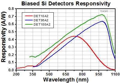
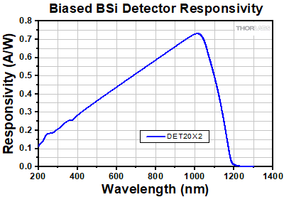
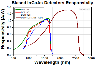
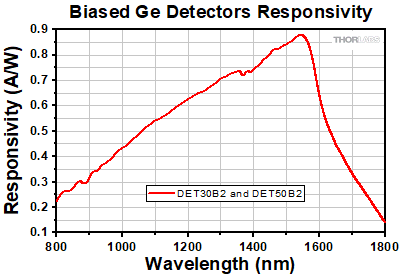


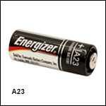
 Zoom
Zoom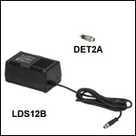


 Free-Space Biased Photodetectors