Free-Space Biased Detectors
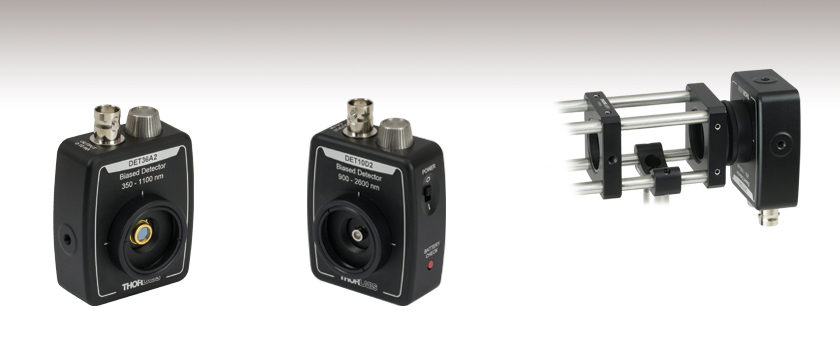
- Monitor CW or Fast Pulsed Lasers
- Detectors for Wavelengths from 200 to 2600 nm
- Integrate with Cage or Lens Tube Systems
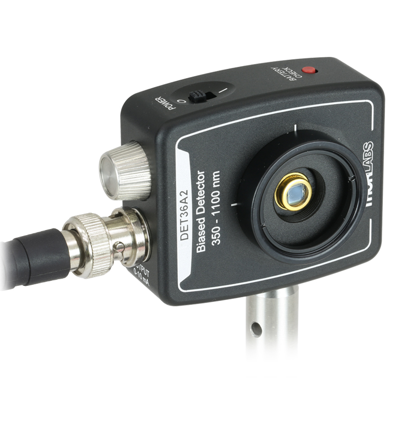
DET36A2
Biased Si Detector
Application Idea
DET Series Detector Attached to a 30 mm Cage System Using the Included SM1 Coupler and an SM1T2 Adapter
(See the Housing Tab for Details)
DET10D2
Biased InGaAs Detector
OVERVIEW
Operating Circuit Diagram

Click to Enlarge
The detectors are reverse biased to produce a linear response with applied input light.

Click to Enlarge
Each detector has an internal SM05 and external SM1 thread and comes with an
attached SM1T1 Internal SM1 Adapter
and SM1RR Retaining Ring.
Features
- Models Covering the 200 nm to 2.6 μm Wavelength Range
- Rise Times as Fast as 1 ns
- Compact Housing for Measurements in Tight Spaces
- SM05 Lens Tube, SM1 Lens Tube, Cage System, and Ø1/2" Post Compatible
- Internal A23 12 V Bias Battery Included
- Optional Power Adapter and Power Supply Available Below
- Can be Fiber Coupled Using Our Internally and Externally SM1-Threaded Fiber Adapters
Thorlabs' Biased Photodetectors are available in models that cover the wavelength range from the UV to the mid-IR (200 nm to 2.6 µm). The slim housing allows the optical detector to slip into tight setups. Our Si and InGaAs detectors are based on fast PIN photodiodes, whereas our Ge detectors are based on N-on-P type photodiodes. Every detector comes complete with an internal bias battery packaged in a rugged aluminum housing. Our biased photodetectors are compatible with our benchtop photodiode amplifier and PMT transimpedance amplifier.
With a wide bandwidth DC-coupled output, these detectors are ideal for monitoring fast pulsed lasers as well as DC optical sources. The direct photodiode anode current is provided on a side panel BNC. This output is easily converted to a positive voltage using a terminating resistor. When looking at high-speed signals, Thorlabs recommends using a 50 Ω load resistor. For lower bandwidth applications, our variable terminator or fixed stub-style terminators quickly adjusts the measured voltage. The detectors below do not have amplifiers or built-in gain, which generally allows them to operate at higher speeds than our PDA series of amplified photodetectors; for applications that require gain or switchable filters, a PDA amplified photodetector may be more suitable.
Click to Enlarge
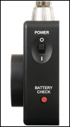
The Red Battery Test Button on the DET10D2
Click to Enlarge
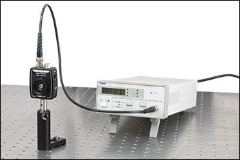
PDA200C Benchtop Photodiode Amplifier Connected to a DET10A2 Photodetector Using a BNC Cable
All connections and controls are located away from the light path, which simplifies integration of our detectors in enclosed spaces. Every detector has internal SM05 (0.535"-40) threading and external SM1 (1.035"-40) threading. Each DET housing includes a detachable Ø1" Optic Mount (Item # SM1T1) that allows for Ø1" optical components, such as optical filters and lenses, to be mounted along the optical axis. Each DET detector can also be mounted in a cage system, lens tube system, or on a Ø1/2" optical post. Every unit's housing features two universal mounting holes that accept both 8-32 and M4 threads. For more information about the location of these mounting points and mounting these units, please see the Housing Features and Mounting Options tabs.
Each detector is reverse-biased by an A23 12 VDC battery incorporated into the housing. The housing also includes a red button (pictured to the left) which, when held down, applies the battery's voltage across the external load. For a high-Z load, this will output the battery's voltage over BNC, providing an easy way to determine if the battery should be replaced without removing it from the housing. An in-line current-limiting resistor prevents fast battery drainage if the battery is tested while connected to a 50 Ω load. Please note that due to slight physical variations of the positive terminal from manufacturer to manufacturer, Thorlabs only recommends using an Energizer® battery in our DET series of photodetectors. A battery was chosen for the reverse bias because it provides an extremely low noise source of power. If the finite lifetime of a battery is not acceptable, the battery can be replaced by a DET2B power adapter bundle. Extra batteries and the DET2B are available for purchase below.
Please note that inhomogeneities at the edges of the active area of the detector can generate unwanted capacitance and resistance effects that distort the time-domain response of the photodiode output. Thorlabs therefore recommends that the incident light on the photodiode is well centered on the active area. The SM1 (1.035"-40) threading on the housing is ideally suited for mounting a Ø1" focusing lens or pinhole in front of the detector element.
Thorlabs also offers high-speed free-space detectors and high-speed fiber-coupled detectors for wavelengths between 400 - 1700 nm.
GRAPHS
HOUSING

Click to Enlarge
All detector housings have a red battery check button. The DET10D2 is shown here.

Click to Enlarge
Each detector has an internal SM05 and external SM1 thread and comes with an
attached SM1T1 Internal SM1 Adapter
and SM1RR Retaining Ring.
DET Series Housing Features
Thorlabs' high-speed detectors feature a slim design. Each housing features internal SM05 (0.535"-40) threading and external SM1 (1.035"-40) threading. Each detector includes an SM1T1 internally SM1-threaded adapter and an SM1RR retaining ring, as shown to the right. The SM1T1 can hold up to 0.1" (2.8 mm) thick optics. The detectors can be mounted using a 1/2" Post, as shown in the images below. Every detector has a housing design that features the active area flush with the front of the housing, simplifying alignments within optomechanical systems. This design also has two universal mounting holes that accept both 8-32 and M4 threads. As a convenience, the back panel is engraved with the responsivity curve of the photodiode.
Lens Tube Compatibility
These detectors can be integrated into various optomechanical systems using the internal SM05 and external SM1 threads. A lens tube can be directly attached to the SM1 threads, making the detectors compatible with lens tube systems. The SM1T1 adapter can be used to mount Ø1" (Ø25.4 mm) optical components, such as optical filters and lenses.
Cage System Compatibility
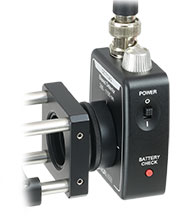
The detectors are also cage system compatible, as shown in the two images below right. A CP33(/M) cage plate can be attached directly to the SM1 threads. This attachment method does not require an adapter piece and allows the diode to be as close as possible to the cage plate, which can be important in setups where the light is divergent. Another method for integrating a detector into a cage system is using the included SM1T1 with an SM1T2 adapter. This allows more freedom in choosing the orientation of the detector. Additionally, these detectors can be used with SM1-threaded fiber adapters (sold below).
Post Mounting
Threaded holes on the housings of the detectors allow the units to be mounted in a horizontal or vertical orientation using a 1/2" Post. This gives the user the option to route the BNC cable from above or alongside the beam path, as shown below left.
Click to Enlarge
DET Photodetector Mounted Horizontally

Click to Enlarge

Click to Enlarge
Click to Enlarge
PIN DIAGRAMS
Output Signal (Photocurrent)
BNC Female
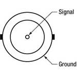
We recommend installing a 50 Ω terminating resistor (e.g., Item # T4119) to the BNC output of each detector. For max photocurrent output, please see the Housing Features column in the tables below.
Note: Our previous generation of free-space biased detectors specified an output voltage, which provided information about the max voltage output under the saturation limit, but the output signal was a photocurrent. To avoid confusion, our current generation of detectors now specify the output current. We apologize for any inconvenience this may have caused.
BATTERY LIFETIME
Battery Lifetime
When using a battery-operated photodetector, it is important to understand the battery’s lifetime and how this affects the operation of the detector. As a current output device, the output current of the photodetector is directly proportional to the amount of incident light on the detector. Most users will convert this current to a voltage by using a terminating load resistor. The resistance value is approximately equal to the circuit gain. For very high speed detectors, such as the DET08 series, it is very important to use a 50 Ω terminating resistor to match the impedance of standard coaxial cables to reduce cable reflections and improve overall signal performance and integrity. Most high-bandwidth scopes come equipped with this termination.
The battery usage lifetime directly correlates to the current used by the detector. Most battery manufacturers provide a battery lifetime in terms of mAh (milliamp hours). For example, if a battery is rated for 190 mA hrs, it will reliably operate for 190 hr at a current draw of 1.0 mA. This battery will be used in the following example on how to determine battery lifetime based on usage.
For this example we have a 780 nm light source with an average 1 mW power is applied to a detector. The responsivity of a biased photodetector based on the response curve at this wavelength is 0.5 A/W. The photocurrent can be calculated as:
![]()
Given the battery has a rated lifetime of 190 mA hr, the battery will last:

or 16 days of continuous use. By reducing the average incident power of the light to 10 µW, the same battery would last for about 4 years when used continuously. When using the recommended 50 Ω terminating load, the 0.5 mA photocurrent will be converted into a voltage of:

If the incident power level is reduced to 40 µW, the output voltage becomes 1 mV. For some measurement devices this signal level may be too low and a compromise between battery life and measurement accuracy will need to be made.
When using a battery-powered, biased photodetector, it is desirable to use as low a light intensity as is possible, keeping in mind the minimum voltage levels required. It is also important to remember that a battery will not immediately cease producing a current as it nears the end of its lifetime. Instead, the voltage of the battery will drop, and the electric potential being applied to the photodiode will decrease. This in turn will increase the response time of the detector and lower its bandwidth. As a result, it is important to make sure the battery has sufficient voltage (as given in the Troubleshooting chapter of the detector's manual) for the detector to operate within its specified parameters. The voltage can be checked with a multimeter.
Another suggestion to increase the battery lifetime is to remove, or power down the light source illuminating the sensor. Without the light source, the photodetector will continue to draw current proportional to the photodetector’s dark current, but this current will be significantly smaller.
For applications where a DET series photodetector is continuously illuminated with a relatively high-power light source, or if having to change the battery is not acceptable, we offer the DET2B power adapter bundle, which includes the power adapter and power supply (sold below). The drawback to this option is the noise in the line voltage will add to the noise in the output signal and could cause more measurement uncertainty.
PHOTODIODE TUTORIAL
Photodiode Tutorial
Theory of Operation
A junction photodiode is an intrinsic device that behaves similarly to an ordinary signal diode, but it generates a photocurrent when light is absorbed in the depleted region of the junction semiconductor. A photodiode is a fast, highly linear device that exhibits high quantum efficiency and may be used in a variety of different applications.
It is necessary to be able to correctly determine the level of the output current to expect and the responsivity based upon the incident light. Depicted in Figure 1 is a junction photodiode model with basic discrete components to help visualize the main characteristics and gain a better understanding of the operation of Thorlabs' photodiodes.

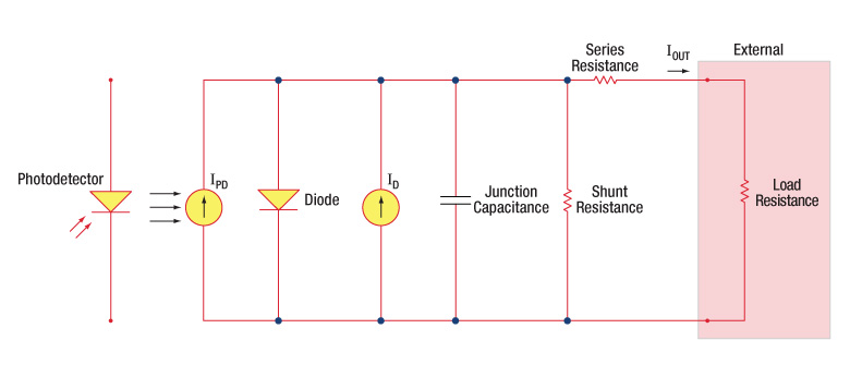
Figure 1: Photodiode Model
Photodiode Terminology
Responsivity
The responsivity of a photodiode can be defined as a ratio of generated photocurrent (IPD) to the incident light power (P) at a given wavelength:

Modes of Operation (Photoconductive vs. Photovoltaic)
A photodiode can be operated in one of two modes: photoconductive (reverse bias) or photovoltaic (zero-bias). Mode selection depends upon the application's speed requirements and the amount of tolerable dark current (leakage current).
Photoconductive
In photoconductive mode, an external reverse bias is applied, which is the basis for our DET series detectors. The current measured through the circuit indicates illumination of the device; the measured output current is linearly proportional to the input optical power. Applying a reverse bias increases the width of the depletion junction producing an increased responsivity with a decrease in junction capacitance and produces a very linear response. Operating under these conditions does tend to produce a larger dark current, but this can be limited based upon the photodiode material. (Note: Our DET detectors are reverse biased and cannot be operated under a forward bias.)
Photovoltaic
In photovoltaic mode the photodiode is zero biased. The flow of current out of the device is restricted and a voltage builds up. This mode of operation exploits the photovoltaic effect, which is the basis for solar cells. The amount of dark current is kept at a minimum when operating in photovoltaic mode.
Dark Current
Dark current is leakage current that flows when a bias voltage is applied to a photodiode. When operating in a photoconductive mode, there tends to be a higher dark current that varies directly with temperature. Dark current approximately doubles for every 10 °C increase in temperature, and shunt resistance tends to double for every 6 °C rise. Of course, applying a higher bias will decrease the junction capacitance but will increase the amount of dark current present.
The dark current present is also affected by the photodiode material and the size of the active area. Silicon devices generally produce low dark current compared to germanium devices which have high dark currents. The table below lists several photodiode materials and their relative dark currents, speeds, spectral ranges, and costs.
| Material | Dark Current | Speed | Spectral Range | Cost |
|---|---|---|---|---|
| Silicon (Si) | Low | High Speed | Visible to NIR | Low |
| Black Silicon (B-Si) | Low | Medium Speeda | Visible to NIR | Moderate |
| Germanium (Ge) | High | Low Speed | NIR | Low |
| Indium Gallium Arsenide (InGaAs) | Low | High Speed | NIR | Moderate |
| Indium Arsenide Antimonide (InAsSb) | High | Low Speed | NIR to MIR | High |
| Extended Range Indium Gallium Arsenide (InGaAs) | High | High Speed | NIR | High |
| Mercury Cadmium Telluride (MCT, HgCdTe) | High | Low Speed | NIR to MIR | High |
Junction Capacitance
Junction capacitance (Cj) is an important property of a photodiode as this can have a profound impact on the photodiode's bandwidth and response. It should be noted that larger diode areas encompass a greater junction volume with increased charge capacity. In a reverse bias application, the depletion width of the junction is increased, thus effectively reducing the junction capacitance and increasing the response speed.
Bandwidth and Response
A load resistor will react with the photodetector junction capacitance to limit the bandwidth. For best frequency response, a 50 Ω terminator should be used in conjunction with a 50 Ω coaxial cable. The bandwidth (fBW) and the rise time response (tr) can be approximated using the junction capacitance (Cj) and the load resistance (RLOAD):

Noise Equivalent Power
The noise equivalent power (NEP) is the input signal power that results in a signal-to-noise ratio (SNR) of 1 in a 1 Hz output bandwidth. This is useful, as the NEP determines the ability of the detector to detect low level light. In general, the NEP increases with the active area of the detector and is given by the following equation:

Here, S/N is the Signal to Noise Ratio, Δf is the Noise Bandwidth, and Incident Energy has units of W/cm2. For more information on NEP, please see Thorlabs' Noise Equivalent Power White Paper.
Terminating Resistance
A load resistance is used to convert the generated photocurrent into a voltage (VOUT) for viewing on an oscilloscope:

Depending on the type of the photodiode, load resistance can affect the response speed. For maximum bandwidth, we recommend using a 50 Ω coaxial cable with a 50 Ω terminating resistor at the opposite end of the cable. This will minimize ringing by matching the cable with its characteristic impedance. If bandwidth is not important, you may increase the amount of voltage for a given light level by increasing RLOAD. In an unmatched termination, the length of the coaxial cable can have a profound impact on the response, so it is recommended to keep the cable as short as possible.
Shunt Resistance
Shunt resistance represents the resistance of the zero-biased photodiode junction. An ideal photodiode will have an infinite shunt resistance, but actual values may range from the order of ten Ω to thousands of MΩ and is dependent on the photodiode material. For example, and InGaAs detector has a shunt resistance on the order of 10 MΩ while a Ge detector is in the kΩ range. This can significantly impact the noise current on the photodiode. For most applications, however, the high resistance produces little effect and can be ignored.
Series Resistance
Series resistance is the resistance of the semiconductor material, and this low resistance can generally be ignored. The series resistance arises from the contacts and the wire bonds of the photodiode and is used to mainly determine the linearity of the photodiode under zero bias conditions.
Common Operating Circuits
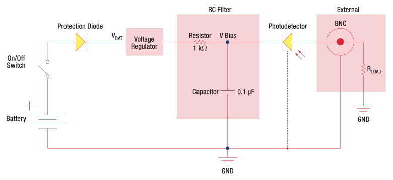
Figure 2: Reverse-Biased Circuit (DET Series Detectors)
The DET series detectors are modeled with the circuit depicted above. The detector is reverse biased to produce a linear response to the applied input light. The amount of photocurrent generated is based upon the incident light and wavelength and can be viewed on an oscilloscope by attaching a load resistance on the output. The function of the RC filter is to filter any high-frequency noise from the input supply that may contribute to a noisy output.
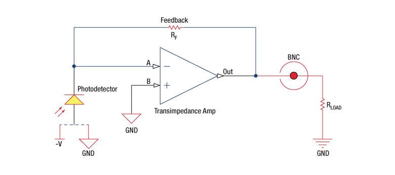
Figure 3: Amplified Detector Circuit
One can also use a photodetector with an amplifier for the purpose of achieving high gain. The user can choose whether to operate in Photovoltaic of Photoconductive modes. There are a few benefits of choosing this active circuit:
- Photovoltaic mode: The circuit is held at zero volts across the photodiode, since point A is held at the same potential as point B by the operational amplifier. This eliminates the possibility of dark current.
- Photoconductive mode: The photodiode is reversed biased, thus improving the bandwidth while lowering the junction capacitance. The gain of the detector is dependent on the feedback element (Rf). The bandwidth of the detector can be calculated using the following:
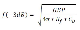
where GBP is the amplifier gain bandwidth product and CD is the sum of the junction capacitance and amplifier capacitance.
Effects of Chopping Frequency
The photoconductor signal will remain constant up to the time constant response limit. Many detectors, including PbS, PbSe, HgCdTe (MCT), and InAsSb, have a typical 1/f noise spectrum (i.e., the noise decreases as chopping frequency increases), which has a profound impact on the time constant at lower frequencies.
The detector will exhibit lower responsivity at lower chopping frequencies. Frequency response and detectivity are maximized for
![]()
LAB FACTS
Dark Current as a Function of Temperature or Reverse-Bias Voltage
Measurements of dark current as a function of temperature and dark current as a function of reverse-bias voltage were acquired for several packaged detectors. As is described in the following section, dark current is a relatively small electrical current that flows in
One set of measurements were taken for silicon (Si), germanium (Ge), and indium gallium arsenide (InGaAs) reverse-biased photodiodes over temperatures from 10 °C to 50 °C, and another set of measurements were taken for the same detectors while they were held at 24 °C and the reverse-bias voltage varied from 0 to 10 V. Please click the "More [+]" labels in the following expandable tables to read about the experiments and our measurements.
Current-Voltage Characteristics of p-n Junction Photodiodes
The characteristic current-voltage relationship of p-n junction photodiodes includes a forward-biased and a reverse-biased voltage regime. Operation of p-n junction photodiodes occurs in the reverse-biased voltage regime, in which a potential difference is applied across the diode to resist the flow of current. A convenient feature of some packaged photodiodes is that a battery inserted into the package can supply the reverse-bias voltage. Ideally, if no light is incident on a reverse-biased photodiode, no current flows.
Under real-world conditions, random processes in the semiconductor material of the photodiode always generate current carriers (electrons and holes) that produce current. These current generation processes are not driven by the photogeneration of electrons and holes. Instead, they are largely driven by the thermal energy contained in the semiconductor material [1]. This dark current is generally small, but it is present when the photodiode is reverse biased and not illuminated. Dark current magnitudes vary for photodiodes of different material compositions; the efficiencies of the thermal generation processes depend on the type and crystal quality of the semiconductor used in the detector's sensing head. The magnitude of the dark current can be expected to increase as the temperature of the photodiode increases and as the reverse-bias voltage applied to the photodiode increases.
It is important to note that if the reverse bias voltage is increased beyond a certain threshold, the photodiode will suffer reverse breakdown, in which the magnitude of the current increases exponentially and permanent damage to the diode is likely. For this reason, many of the Thorlabs DET packages include a voltage regulator to prevent the bias voltage from reaching breakdown.
When a photodiode is illuminated, the current generated by the incident light adds to the dark current. The carriers in the photocurrent are generated by the energy contained in the photons of the incident light. Above a certain illumination threshold intensity, the magnitude of the photocurrent exceeds the magnitude of the dark current. When the photocurrent is larger than the dark current, the magnitude of the photocurrent can be calculated by measuring the total current and then subtracting the contribution of the dark current. When the photocurrent is smaller than the noise on the dark current, the photocurrent is undetectable. Because of this, it is desirable to minimize the levels of dark current in photodiodes.
[1] J. Liu, Photonic Devices. Cambridge University Press, Cambridge, UK, 2005
| Dark Current as a Function of Temperature |
|---|
|
Dark currents were measured over temperatures of 10 °C to 50 °C for three representative packaged detectors: the Si-based DET100A (previous generation), the Ge-based DET50B (previous generation), and the InGaAs-based DET10C (previous generation).  Click to Enlarge Figure 1: The Nested Metal Box Test Fixture with Covers Removed and DET10C Installed Black insulating foam lines the interiors of both boxes. A: Outer Aluminum Box; B: Inner Aluminum Box; C: Thermistor; D: DET10C; E: BNC-to-Triax Feedthrough; F: BNC-to-BNC Feedthrough Experimental Setup As the dark current depends to some degree on the magnitude of the reverse-bias voltage, care was taken to ensure the reverse-bias voltage remained constant over the duration of each measurement set. For these detectors, the source of the reverse-bias voltage was a battery. Before each data set was acquired, the detector's A23 battery was replaced with a fresh one. The battery's voltage was also measured before and after each test to ensure the bias voltage remained constant over the course of the measurement. Thermistors were used to monitor the temperatures of each photodiode continuously during the experiment. A thermistor was held in contact with the outer surface of the TO can housing using a piece of thermal tape. With the thermistor in place, it was not possible to use the detector cap to block light from reaching the photodiode. The detector enclosure consisted of a pair of nested aluminum metal boxes, which are shown with their covers off in Figure 1. Only one box would be required to create a light-tight environment for the photodiode, but an outer box was included in the setup to shield the inner box from EMI related noise. The detector was placed inside the inner box, which was equipped with a BNC-to-triax adapter feedthrough; the BNC end was accessible from the inside of the box, and the triax end was accessible from the outside of the box. The BNC connector on the detector was attached directly to the BNC end of the adapter, which advantageously eliminated the need to use a BNC cable. BNC cables are poorly shielded, and using one could introduce noise from EMI sources to the signal read from the detector. This inner metal box was placed inside of an outer metal box, which possessed a triax-to-triax feedthrough. A triax cable was used to route the detector signal between the feedthroughs on the inner and outer boxes. A triax cable was also used to connect the Keithley 6487 ammeter to the end of the Triax-to-Triax feedthrough accessible on the outside of the outer box. The outer metal box served to isolate the inner metal box from EMI, and the triax cables shielded the detector signal from EMI. After covering two boxes with their respective lids, the nested box set was placed inside an ESPEC ESX-3CW temperature chamber. The ammeter was located outside of the chamber. The electrical connection between the thermistor and TSP01 temperature logger was performed using BNC cables, BNC-to-BNC bulkhead feedthroughs to route the signal out of the nested boxes, and a custom BNC-to-phono jack cable to connect to the temperature logger. Experimental Results The data curves plotted in Figure 2 show the InGaAs-based detector exhibited the least amount of dark current and the Ge-based detector exhibited the most, with the levels of the latter being approximately 5 orders of magnitude higher. In all cases, the dark current increased with the temperature of the photodiode, as expected. The individual points on this graph, plotted as diamonds, are the values of the dark current specified for each detector at 25 °C. These points specify a maximum value of dark current at 25 °C; each diode's dark current must be equal to or less than this value at 25 °C, but the dark current may exceed this specification at higher temperatures, as is the case for the measured DET50B detector. 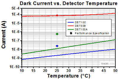 Click to Enlarge Figure 2: Dark Current Data Measured for Three Packaged Photodiodes The discrete data points, plotted as diamonds, are values of the dark current specified for each detector at 25 °C.  Click to Enlarge Figure 3: Temperature of a Representative Photodiode Controlled by the Conditions in the Environmental Chamber Dark current measurements were acquired between 10 °C and 50 °C (indicated by the shaded region) and are plotted in Figure 2 . Experimental Limitations |
| Dark Current as a Function of Reverse-Bias Voltage |
|---|
|
Dark currents were measured while three representative packaged detectors, the Si-based DET100A (previous generation), the Ge-based DET50B (previous generation), and the InGaAs-based DET10C (previous generation), were held at 24 °C and their reverse-bias voltages were varied between 0 and 10 V. Either a battery or an external power supply, such as the DET2B Power Adapter Bundle, can be used to provide the required reverse-bias voltage. The measurements described below were made to demonstrate the change in dark current as the voltage supplied by the battery decreases from battery drainage.  Click to Enlarge Figure 1: The Nested Metal Box Test Fixture with Covers Removed and DET10C Installed Black insulating foam lines the interiors of both boxes. A: Outer Aluminum Box; B: Inner Aluminum Box; C: Thermistor; D: DET10C; E: Power Adapter of the DET1B Power Supply; F: BNC-to-BNC Feedthrough for the DET1B, G: BNC-to-Triax Feedthrough for the Detector Signal; H: BNC-to-BNC Feedthrough for the Thermistor Experimental Setup The detector enclosure consisted of a pair of nested aluminum metal boxes, which are shown with their covers off in Figure 1. Only one box would be required to create a light-tight environment for the photodiode, but an outer box was included in the setup to shield the inner box from EMI related noise. The detector was placed inside the inner box, and electrical connections were made through it using BNC and BNC-to-triax adapter feedthroughs. The measurement signal from the detector was routed through the BNC-to-triax adapter feedthrough. The BNC connector on the detector was attached directly to the BNC end of the adapter, which advantageously eliminated the need to use a BNC cable. BNC cables are poorly shielded, and using one could introduce noise from EMI sources to the signal read from the detector. This inner metal box was placed inside of an outer metal box, which possessed a triax-to-triax feedthrough. A triax cable was used to route the detector signal between the feedthroughs on the inner and outer boxes. A triax cable was also used to connect the Keithley 6487 ammeter to the end of the Triax-to-Triax feedthrough accessible on the outside of the outer box. The outer metal box served to isolate the inner metal box from EMI, and the triax cables shielded the detector signal from EMI. After covering the two boxes with their respective lids, the nested box set was placed inside an ESPEC ESX-3CW temperature chamber. The ammeter was located outside of the chamber. A DET1B (previous generation, current generation DET2B), which includes a power supply and a power adapter designed to be inserted into the battery port of the DET series detectors, was used to supply the reverse-bias voltage, which was routed through BNC feedthroughs. The power adapter was inserted into the detector, and the opposite end of the adapter was connected to a BNC feedthrough fitted into the wall of the inner box. A BNC cable and another feedthrough were used to extend the electrical connection to the outside of the outer box, and the voltage output of the Keithley 6487 was connected to that. A computer was interfaced with the Keithley, which allowed the computer to simultaneously control the reverse-bias voltage while measuring the dark current. As the dark current depends strongly on temperature, thermistors were used to monitor the temperatures of each photodiode continuously during the experiment. A thermistor was held in contact with the outer surface of the TO can housing using a piece of thermal tape. With the thermistor in place, it was not possible to use the detector cap to block light from reaching the photodiode. The electrical connection between the thermistor and TSP01 temperature logger was performed using BNC cables, BNC-to-BNC bulkhead feedthroughs to route the signal out of the nested boxes, and a custom BNC-to-phono jack cable to connect to the temperature logger. Experimental Results The Si-based DET100A does not contain an integrated voltage regulator, while both the Ge-based DET50B and the InGaAs-based DET10C do. Voltage regulators integrated into photodiodes are used to maintain a stable reverse bias voltage across the photodiode. In general, voltage regulators are applied in a range of applications to automatically maintain a stable voltage level: the regulator ensures that the output voltage level is approximately constant as long as the voltage input falls within a specified range. When the input voltage decreases below the voltage regulator's dropout voltage, which marks the lower end of the range, the regulator is no longer able to regulate the output voltage. As the input voltage continues to decrease from the dropout voltage, the output voltage decreases until a threshold is reached and the regulator becomes non-functional. While in this off state, the output voltage is negligible. In the case of the Ge-based DET50B and the InGaAs-based DET10C, the output voltage provided by the voltage regulator is used to reverse bias the photodiode. The absence of a voltage regulator in the Si-based DET100A results in its measured dark current, plotted in Figure 2, continuing to increase as the voltage supplied by the Keithley 6487 increases. The dark current measured for the DET100A increases exponentially up to a reverse-bias voltage of 0.5 V, and then it increases linearly for reverse-bias voltages between approximately 0.5 V and 10 V. A fresh battery supplies ≥10 V. Both the Ge-based DET50B, shown in Figure 3, and the InGaAs-based DET10C, shown in Figure 4, exhibit no dark current until the reverse-bias voltage reaches a threshold (approximately 1 V for the DET50B and 1.5 V for the DET10C). The voltage range up to this threshold value corresponds to the off state of the voltage regulator. After this threshold is exceeded, the dark currents measured for these detectors increase, approximately exponentially, until the voltage supplied by the Keithley 6487 reaches the dropout regulator voltage of 5.5 V. For supplied voltages between 5.5 V and 10 V, the voltage regulator maintains a constant 5.5 V reverse-bias across the photodiodes, which results in an approximately constant values of dark current for supplied voltages over this range. As a fresh battery supplies ≥10 V, the voltage regulator has the effect of ensuring the dark current level remains approximately constant over much of the battery's lifetime, as well as protecting the photodiode from exposure to excessive reverse-bias voltages in general.  Click to Enlarge Figure 2: Dark current data measured for the Si-based DET100A packaged photodiode, which does not include an integrated voltage regulator, is plotted as a function of the voltage supplied by the Keithley 6487. 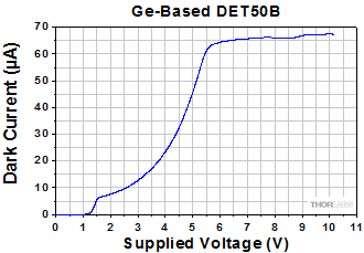 Click to Enlarge Figure 3: Dark current data measured for the Ge-based DET50B packaged photodiode, which includes an integrated voltage regulator, is plotted as a function of the voltage supplied by the Keithley 6487. 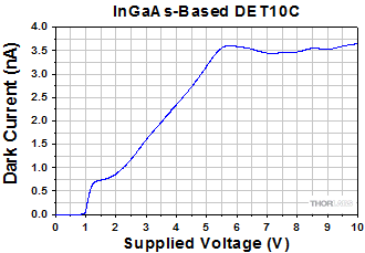 Click to Enlarge Figure 4: Dark current data measured for the InGaAs-Based DET10C packaged photodiode, which includes an integrated voltage regulator, is plotted as a function of the voltage supplied by the Keithley 6487. Experimental Limitations |
About Our Lab Facts
Our application engineers live the experience of our customers by conducting experiments in Alex’s personal lab. Here, they gain a greater understanding of our products’ performance across a range of application spaces. Their results can be found throughout our website on associated product pages in Lab Facts tabs. Experiments are used to compare performance with theory and look at the benefits and drawbacks of using similar products in unique setups, in an attempt to understand the intricacies and practical limitations of our products. In all cases, the theory, procedure, and results are provided to assist with your buying decisions.
PREVIOUS GENERATION 
The following table lists Thorlab's selection of previous and current generation PDA, PDF, and DET detectors.
| Previous Generation Cross Reference of PDA and DET Detectors | |||||
|---|---|---|---|---|---|
| Wavelength | Material | Biased Detector |
Amplified Detector |
||
| Current Generation | Previous Generation | Current Generation | Previous Generation | ||
| 200 - 1100 nm | Si | DET10A2 | DET10A(/M) | PDA10A2 | PDA10A(-EC) |
| 320 - 1000 nm | Si | - | - | PDA8A2 | PDA8A |
| 400 - 1000 nm | Si | - | - | PDA015A2 | PDA015A(/M) |
| 320 - 1100 nm | Si | DET100A2 | DET100A(/M)a | PDA100A2 | PDA100A(-EC)b |
| Si | - | - | PDF10A2 | PDF10A(/M) | |
| 350 - 1100 nm | Si | DET36A2 | DET36A(/M) | PDA36A2 | PDA36A(-EC) |
| 500 - 1700 nm | InGaAs | DET10N2 | DET10N(/M) | - | - |
| 800 - 1700 nm | InGaAs | DET20C2 | DET20C(/M) | PDA20CS2 | PDA20CS(-EC) |
| - | - | PDA05CF2 | PDA10CF(-EC) | ||
| - | - | PDA015C2 | PDA015C(/M) | ||
| - | - | PDF10C2 | PDF10C(/M) | ||
| - | - | PDA20C2 | PDA20C(/M) | ||
| 800 - 1800 nm | Ge | DET30B2 | DET30B(/M) | PDA30B2 | PDA30B(-EC) |
| DET50B2 | DET50B(/M) | PDA50B2 | PDA50B(-EC) | ||
| 900 - 1700 nm | InGaAs | DET10C2 | DET10C(/M) | PDA10CS2 | PDA10CS(-EC) |
| 900 - 2600 nm | InGaAs | DET05D2 | DET05D(/M)c | PDA10D2 | PDA10D(-EC)c |
| DET10D2 | DET10D(/M)c | - | - | ||
PULSE CALCULATIONS
Pulsed Laser Emission: Power and Energy Calculations
Determining whether emission from a pulsed laser is compatible with a device or application can require referencing parameters that are not supplied by the laser's manufacturer. When this is the case, the necessary parameters can typically be calculated from the available information. Calculating peak pulse power, average power, pulse energy, and related parameters can be necessary to achieve desired outcomes including:
- Protecting biological samples from harm.
- Measuring the pulsed laser emission without damaging photodetectors and other sensors.
- Exciting fluorescence and non-linear effects in materials.
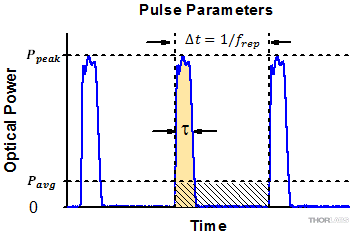
Pulsed laser radiation parameters are illustrated in Figure 1 and described in the table. For quick reference, a list of equations is provided below. The document available for download provides this information, as well as an introduction to pulsed laser emission, an overview of relationships among the different parameters, and guidance for applying the calculations.
|
Equations: |
||||
 |
and |  |
||
 |
||||
 |
||||
 |
||||
Peak power and average power calculated from each other: |
||||
 |
and |  |
||
| Peak power calculated from average power and duty cycle*: | ||||
 |
*Duty cycle ( ) is the fraction of time during which there is laser pulse emission. ) is the fraction of time during which there is laser pulse emission. |
|||
Click to Enlarge
Figure 1: Parameters used to describe pulsed laser emission are indicated in the plot (above) and described in the table (below). Pulse energy (E) is the shaded area under the pulse curve. Pulse energy is, equivalently, the area of the diagonally hashed region.
| Parameter | Symbol | Units | Description | ||
|---|---|---|---|---|---|
| Pulse Energy | E | Joules [J] | A measure of one pulse's total emission, which is the only light emitted by the laser over the entire period. The pulse energy equals the shaded area, which is equivalent to the area covered by diagonal hash marks. | ||
| Period | Δt | Seconds [s] | The amount of time between the start of one pulse and the start of the next. | ||
| Average Power | Pavg | Watts [W] | The height on the optical power axis, if the energy emitted by the pulse were uniformly spread over the entire period. | ||
| Instantaneous Power | P | Watts [W] | The optical power at a single, specific point in time. | ||
| Peak Power | Ppeak | Watts [W] | The maximum instantaneous optical power output by the laser. | ||
| Pulse Width |  |
Seconds [s] | A measure of the time between the beginning and end of the pulse, typically based on the full width half maximum (FWHM) of the pulse shape. Also called pulse duration. | ||
| Repetition Rate | frep | Hertz [Hz] | The frequency with which pulses are emitted. Equal to the reciprocal of the period. | ||
Example Calculation:
Is it safe to use a detector with a specified maximum peak optical input power of 75 mW to measure the following pulsed laser emission?
- Average Power: 1 mW
- Repetition Rate: 85 MHz
- Pulse Width: 10 fs
The energy per pulse:

seems low, but the peak pulse power is:

It is not safe to use the detector to measure this pulsed laser emission, since the peak power of the pulses is >5 orders of magnitude higher than the detector's maximum peak optical input power.
CROSS REFERENCE
The following table lists Thorlabs' selection of photodiodes, photoconductive, and pyroelectric detectors. Item numbers in the same row contain the same detector element.
Biased Si Detectors: 200 - 1100 nm
| Item #a | Housing Features |
Active Area |
Wavelength Range |
Rise Timeb,c,d |
Bandwidth | Noise-Equivalent Power (NEP) (Typ.) |
Dark Currente |
Junction Capacitance |
Bias Voltage |
Responsivity Plotf (Raw Data) |
|---|---|---|---|---|---|---|---|---|---|---|
| DET10A2 | 0.8 mm2 (Ø1.0 mm)g |
200 - 1100 nmh | 1 ns (Typ.) | 350 MHzi | 5.0 x 10⁻¹⁴ W/Hz1/2 |
0.3 nA (Typ.) 2.5 nA (Max) |
6 pF (Typ.) | 10 V | ||
| DET100A2 | 75.4 mm2 (Ø9.8 mm) |
320 - 1100 nm | 35 nsj (Typ.) | 10 MHzk | 2.4 x 10⁻¹⁴ W/Hz1/2 | 0.9 nA (Typ.) 10 nA (Max) |
150 pF (Typ.) | 10 V | ||
| DET36A2 |  |
13 mm2 (3.6 x 3.6 mm)g |
350 - 1100 nm | 14 nsj (Typ.) | 25 MHzk | 1.6 x 10⁻¹⁴ W/Hz1/2 | 0.35 nA (Typ.) 6.0 nA (Max) |
40 pF (Typ.) | 10 V |
Part Number | Description | Price | Availability |
|---|---|---|---|
DET10A2 | Si Detector, 200 - 1100 nm, 1 ns Rise Time, 0.8 mm², Universal 8-32 / M4 Mounting Holes | $181.68 | 3 Weeks |
DET100A2 | Si Detector, 320 - 1100 nm, 35 ns Rise Time, 75.4 mm², Universal 8-32 / M4 Mounting Holes | $191.26 | Today |
DET36A2 | Si Detector, 350 - 1100 nm, 14 ns Rise Time, 13 mm², Universal 8-32 / M4 Mounting Holes | $140.91 | Today |
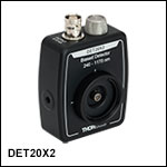
Biased Black-Silicon Detector: 240 - 1170 nm
| Item #a | Housing Features |
Active Area |
Wavelength Rangeb |
Rise / Fall Timeb,c,d |
Bandwidthe | Noise-Equivalent Power (NEP) (Typ.)f |
Dark Currentg |
Junction Capacitance |
Bias Voltage |
Responsivity Plot (Raw Data) |
|---|---|---|---|---|---|---|---|---|---|---|
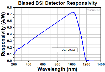
| DET20X2 |  |
4 mm2 (2 x 2 mm)h |
240 - 1170 nm | 15 ns / 29 ns (Typ.) | 23.3 MHz | 7.1 x 10⁻¹⁵ W/Hz1/2 | 50 pA (Typ.) 1 nA (Max) |
13 pF (Typ.) | 10 V |
Part Number | Description | Price | Availability |
|---|---|---|---|
DET20X2 | Customer Inspired! B-Si Detector, 240 - 1170 nm, 15 ns Rise Time, 4 mm², Universal 8-32 / M4 Mounting Holes | $361.01 | 3 Weeks |
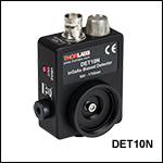
Biased InGaAs Detectors: 500 - 2600 nm
| Item #a | Housing Features |
Active Area |
Wavelength Range |
Rise Timeb,c |
Bandwidthd | Noise-Equivalent Power (NEP) (Typ.) |
Dark Currente |
Junction Capacitance |
Bias Voltage |
Responsivity Plot (Raw Data) |
|---|---|---|---|---|---|---|---|---|---|---|
| DET10N2 |  |
0.8 mm2 (Ø1.0 mm)f |
500 - 1700 nm | 5 nsg (Typ.) |
70 MHz | 2.0 x 10⁻¹⁴ W/Hz1/2 | 1.5 nA (Typ.) 10 nA (Max) |
50 pF (Typ.) | 5.0 V | |
| DET20C2 |  |
3.14 mm2 (Ø2.0 mm)f |
800 - 1700 nm | 30 nsh (Typ.) |
11.7 MHz | 1.3 x 10⁻¹³ W/Hz1/2 | 55 nA (Typ.) 200 nA (Max) |
100 pF (Typ.) | 1.8 V | |
| DET10C2 | 0.8 mm2 (Ø1.0 mm)f |
900 - 1700 nm | 10 nsg (Typ.) |
35 MHz | 2.5 x 10⁻¹⁴ W/Hz1/2 | 1 nA (Typ.) 25 nA (Max) |
80 pF (Typ.) | 5.0 V | ||
| DET05D2 | 0.2 mm2 (Ø0.5 mm)f |
900 - 2600 nm | 17 nsh (Typ.) |
20.6 MHz | 1.0 x 10⁻¹² W/Hz1/2 | 2 µA (Typ.) 20 µA (Max) |
140 pF (Typ.) | 1.8 V | ||
| DET10D2 | 0.8 mm2 (Ø1.0 mm)f |
900 - 2600 nm | 25 nsh (Typ.) |
14 MHz | 1.5 x 10⁻¹² W/Hz1/2 | 5 µA (Typ.) 40 µA (Max) |
500 pF (Typ.) | 1.8 V |
Part Number | Description | Price | Availability |
|---|---|---|---|
DET10N2 | InGaAs Detector, 500 - 1700 nm, 5 ns Rise Time, 0.8 mm², Universal 8-32 / M4 Mounting Holes | $597.53 | Today |
DET20C2 | InGaAs Detector, 800 - 1700 nm, 30 ns Rise Time, 3.14 mm², Universal 8-32 / M4 Mounting Holes | $482.30 | Today |
DET10C2 | InGaAs Detector, 900 - 1700 nm, 10 ns Rise Time, 0.8 mm², Universal 8-32 / M4 Mounting Holes | $352.81 | Today |
DET05D2 | InGaAs Detector, 900 - 2600 nm, 17 ns Rise Time, 0.2 mm², Universal 8-32 / M4 Mounting Holes | $437.16 | Today |
DET10D2 | InGaAs Detector, 900 - 2600 nm, 25 ns Rise Time, 0.8 mm², Universal 8-32 / M4 Mounting Holes | $511.99 | Today |
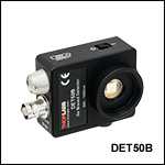
Biased Ge Detectors: 800 - 1800 nm
| Item #a | Housing Features |
Active Area |
Wavelength Range |
Rise Timeb,c | Bandwidthd | Noise-Equivalent Power (NEP) (Typ.) |
Dark Currente |
Junction Capacitance |
Bias Voltage |
Responsivity Plot (Raw Data) |
|---|---|---|---|---|---|---|---|---|---|---|
| DET50B2 | 19.6 mm2 (Ø5.0 mm)f |
800 - 1800 nm | 455 nsg (Typ.) |
770 kHz | 4.0 x 10⁻¹² W/Hz1/2 | 40 µA (Typ.) 80 µA (Max) |
4000 pF (Max) | 5.0 V | ||
| DET30B2 | 7.1 mm2 (Ø3.0 mm)f |
800 - 1800 nm | 650 nsh (Typ.) |
540 kHz | 2.6 x 10⁻¹² W/Hz1/2 | 4.0 µA (Max) | 6 nF (Max) | 1.8 V |
Part Number | Description | Price | Availability |
|---|---|---|---|
DET50B2 | Ge Detector, 800 - 1800 nm, 455 ns Rise Time, 19.6 mm², Universal 8-32 / M4 Mounting Holes | $496.55 | Today |
DET30B2 | Ge Detector, 800 - 1800 nm, 650 ns Rise Time, 7.1 mm², Universal 8-32 / M4 Mounting Holes | $361.12 | Today |
Replacement Battery for Photodetectors

The A23 is a replacement alkaline battery for Thorlabs' DET photodetectors. For cases where the finite lifetime of a battery is not acceptable, we also offer an AC power adapter; please see below for more information. Information on expected battery lifetime is in the Battery Lifetime tab above.
Part Number | Description | Price | Availability |
|---|---|---|---|
A23 | Replacement 12 V Alkaline Battery for DET Series | $5.85 | Today |
DET Power Adapter
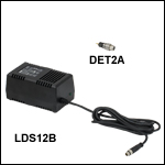
- DET2A: Power Adapter for DET Series Detectors
- LDS12B: ±12 VDC Power Supply
- DET2B: Bundle of the DET2A and LDS12B
DET2A Power Adapter
The DET2A is a power adapter for our DET series detectors. This power adapter will directly replace the A23 battery and spring-loaded cap to allow the detector to run directly from our LDS12B power supply (sold separately). The DET2A is also compatible with the PDA-C-72 power supply cable for custom connections. Note that when connecting the DET2A and the PDA-C-72 to power DET series detectors, only the brown (+12 V) and black (GND) pins are needed.
LDS12B Power Supply
The LDS12B is a ±12 VDC regulated power supply, which incorporates a current limit, enabling short circuit and overload protection; an on/off switch with an LED indicator; and a switchable AC input voltage (100, 120, or
230 VAC). A region-specific power cord is shipped with the LDS12B power supply based on your location.
DET2B Power Adapter Bundle
The DET2B power adapter bundle includes both the DET2A power adapter and the LDS12B power supply. This power adapter bundle can be used to replace the battery in our DET series detectors. To use the DET2B, simply replace the battery and spring-loaded cap with the included DET2A adapter, insert the three pin plug from the LDS12B power supply into the adapter, and screw the adapter into the detector. This procedure is depicted in the animation to the above right.
Part Number | Description | Price | Availability |
|---|---|---|---|
DET2A | DET Power Adapter | $46.01 | Lead Time |
LDS12B | ±12 VDC Regulated Linear Power Supply, 6 W, 100/120/230 VAC | $93.55 | Today |
DET2B | DET Power Adapter & Power Supply Bundle | $137.43 | Today |
Internally SM1-Threaded Fiber Adapters
- FC/PC (Narrow or Wide Key), FC/APC (Narrow Key or Wide Key), SMA, ST®*/PC, SC/PC, LC/PC, or Ø2.5 mm Ferrule Receptacles
- Light-Tight Construction When Used with SM1 Lens Tubes
- Compatible with Many of Our Photodiode Power Sensors
Note: The APC adapters have two dimples in the front surface that allow them to be tightened with the SPW909 or SPW801 spanner wrench. The dimples do not go all the way through the disk so that the adapter can be used in light-tight applications when paired with SM1 lens tubes.
FC/PC and FC/APC adapters are available with either narrow (2.0 mm) or wide (2.2 mm) key connectors; for more details on narrow versus wide key connectors, please see our Intro to Fiber tutorial.
The S120-25 ferrule adapter is designed without a locking connector mechanism and accepts fiber patch cables with Ø2.5 mm ferrules for quick measurements with photodetectors or power sensors.
*ST® is a registered trademark of Lucent Technologies, Inc.
Part Number | Description | Price | Availability |
|---|---|---|---|
S120-FC2 | FC/PC Fiber Adapter Cap with Internal SM1 (1.035"-40) Threads, Narrow Key (2.0 mm) | $46.33 | Today |
S120-FC | FC/PC Fiber Adapter Cap with Internal SM1 (1.035"-40) Threads, Wide Key (2.2 mm) | $46.33 | Today |
S120-APC2 | FC/APC Fiber Adapter Cap with Internal SM1 (1.035"-40) Threads, Narrow Key (2.0 mm) | $36.18 | Today |
S120-APC | Customer Inspired! FC/APC Fiber Adapter Cap with Internal SM1 (1.035"-40) Threads, Wide Key (2.2 mm) | $36.18 | Today |
S120-SMA | SMA Fiber Adapter Cap with Internal SM1 (1.035"-40) Threads | $46.33 | Today |
S120-ST | ST/PC Fiber Adapter Cap with Internal SM1 (1.035"-40) Threads | $46.33 | Today |
S120-SC | SC/PC Fiber Adapter Cap with Internal SM1 (1.035"-40) Threads | $58.21 | Today |
S120-LC | LC/PC Fiber Adapter Cap with Internal SM1 (1.035"-40) Threads | $58.21 | Today |
S120-25 | Customer Inspired! Ø2.5 mm Ferrule Adapter Cap with Internal SM1 (1.035"-40) Threads | $46.33 | Today |
Externally SM1-Threaded Fiber Adapters
- FC/PC (Narrow or Wide Key), FC/APC (Narrow or Wide Key), SMA, ST®*/PC, SC/PC, or LC/PC Receptacles
- Vacuum-Compatible Versions of FC/PC Wide-Key and SMA Receptacles Available
- Light-Tight When Used with SM1 Lens Tubes
- Compatible with Many of Our 30 mm Cage Plates and Photodetectors
Note: Each disk has four dimples, two in the front surface and two in the back surface, that allow it to be tightened from either side with the SPW909 or SPW801 spanner wrench. The dimples do not go all the way through the disk so that the adapters can be used in light-tight applications when paired with SM1 lens tubes. Once the adapter is at the desired position, use an SM1RR retaining ring to secure it in place.
FC/PC and FC/APC adapters are available with either narrow (2.0 mm) or wide (2.2 mm) key connectors; for more details on narrow versus wide key connectors, please see our Intro to Fiber tutorial.
*ST® is a registered trademark of Lucent Technologies, Inc.
Part Number | Description | Price | Availability |
|---|---|---|---|
SM1FC2 | FC/PC Fiber Adapter Plate with External SM1 (1.035"-40) Threads, Narrow Key (2.0 mm) | $34.45 | Today |
SM1FC | FC/PC Fiber Adapter Plate with External SM1 (1.035"-40) Threads, Wide Key (2.2 mm) | $34.45 | Today |
SM1FCV | Vacuum-Compatible FC/PC Fiber Adapter Plate with External SM1 (1.035"-40) Threads, Wide Key (2.2 mm) | $76.17 | Today |
SM1FCA2 | Customer Inspired! FC/APC Fiber Adapter Plate with External SM1 (1.035"-40) Threads, Narrow Key (2.0 mm) | $36.54 | Today |
SM1FCA | FC/APC Fiber Adapter Plate with External SM1 (1.035"-40) Threads, Wide Key (2.2 mm) | $36.54 | Today |
SM1SMA | SMA Fiber Adapter Plate with External SM1 (1.035"-40) Threads | $33.61 | Today |
SM1SMAV | Vacuum-Compatible SMA Fiber Adapter Plate with External SM1 (1.035"-40) Threads | $60.14 | Today |
SM1ST | ST/PC Fiber Adapter Plate with External SM1 (1.035"-40) Threads | $32.04 | Today |
SM1SC1 | SC/PC Fiber Adapter Plate with External SM1 (1.035"-40) Threads | $65.58 | Today |
SM1LC | LC/PC Fiber Adapter Plate with External SM1 (1.035"-40) Threads | $65.58 | Today |


